Supercharge Your Innovation With Domain-Expert AI Agents!

Method for producing reconstituted wafers with support of the chips during their encapsulation

a technology of reconstituted wafers and chips, applied in the direction of ion implantation coating, chemical vapor deposition coating, coating, etc., can solve the problems of more or less isotropic and unforeseeable, limit of this technique, and not being able to eliminate, so as to reduce the drawback of chip displacement

Active Publication Date: 2015-08-18
3D PLUS
View PDF16 Cites 1 Cited by
  • Summary
  • Abstract
  • Description
  • Claims
  • Application Information

AI Technical Summary

Benefits of technology

The invention aims to solve the issue of chips shifting during resin encapsulation without resorting to steps of sticking and damaging the grid. The patent proposes a technique called "Atmospheric plasma deposition" which is a non-vacuum process for chemical vapor deposition at low temperatures. This technique has advantages, such as excellent adhesion because the plasma makes the surface clean before deposition.

Problems solved by technology

An evident drawback is the displacement of the chips during the deposition of the resin and / or during its polymerization, the pads of the chips then no longer coinciding with the tracks of the redistribution layer (RDL layer).
This results in more or less isotropic and unforeseeable micro displacements, typically of between a few μm and a few tens of μm, this possibly exceeding the positioning (with respect to the RDL layer) tolerances required after molding, which are typically of the order of 10 μm.
One of the limits of this technique stems from the fact that the micro displacements are not all foreseeable, notably those of the various types of chips within one and the same pattern.
This method makes it possible to reduce the expansion and therefore the displacement of the chips but does not make it possible to eliminate it since this does not resolve the problem of the tacky skin which likewise moves.
It furthermore exhibits the following drawbacks:the lattice necessarily remains in the final package since once molded in the resin, it can no longer be removed,this limits the number of chips on the wafer on account of the significant space taken up by the lattice,this requires double slicing to eliminate the bars of the lattice,the correction of the masks and therefore of the position of the conducting tracks of the redistribution layers can impede the subsequent stacking of the reconstituted wafers which require a rigorously constant spacing by construction.
For the most critical cases, chip-by-chip irradiation is carried out, this being very expensive and not making it possible to guarantee the spacing for the stacking steps.
The only drawbacks of this technique are due to the fact that additional steps of sticking and of destroying the provisional grid are necessary.

Method used


Image

  • Method for producing reconstituted wafers with support of the chips during their encapsulation
  • Method for producing reconstituted wafers with support of the chips during their encapsulation
  • Method for producing reconstituted wafers with support of the chips during their encapsulation

Examples


Embodiment Construction

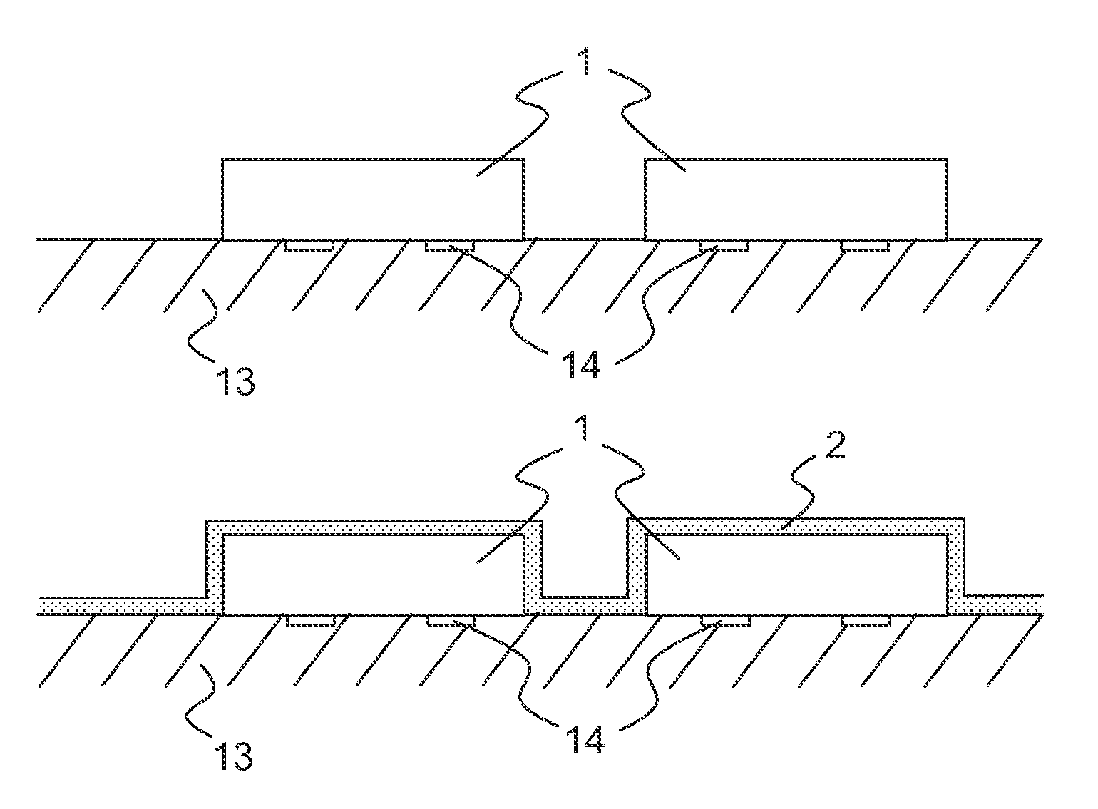
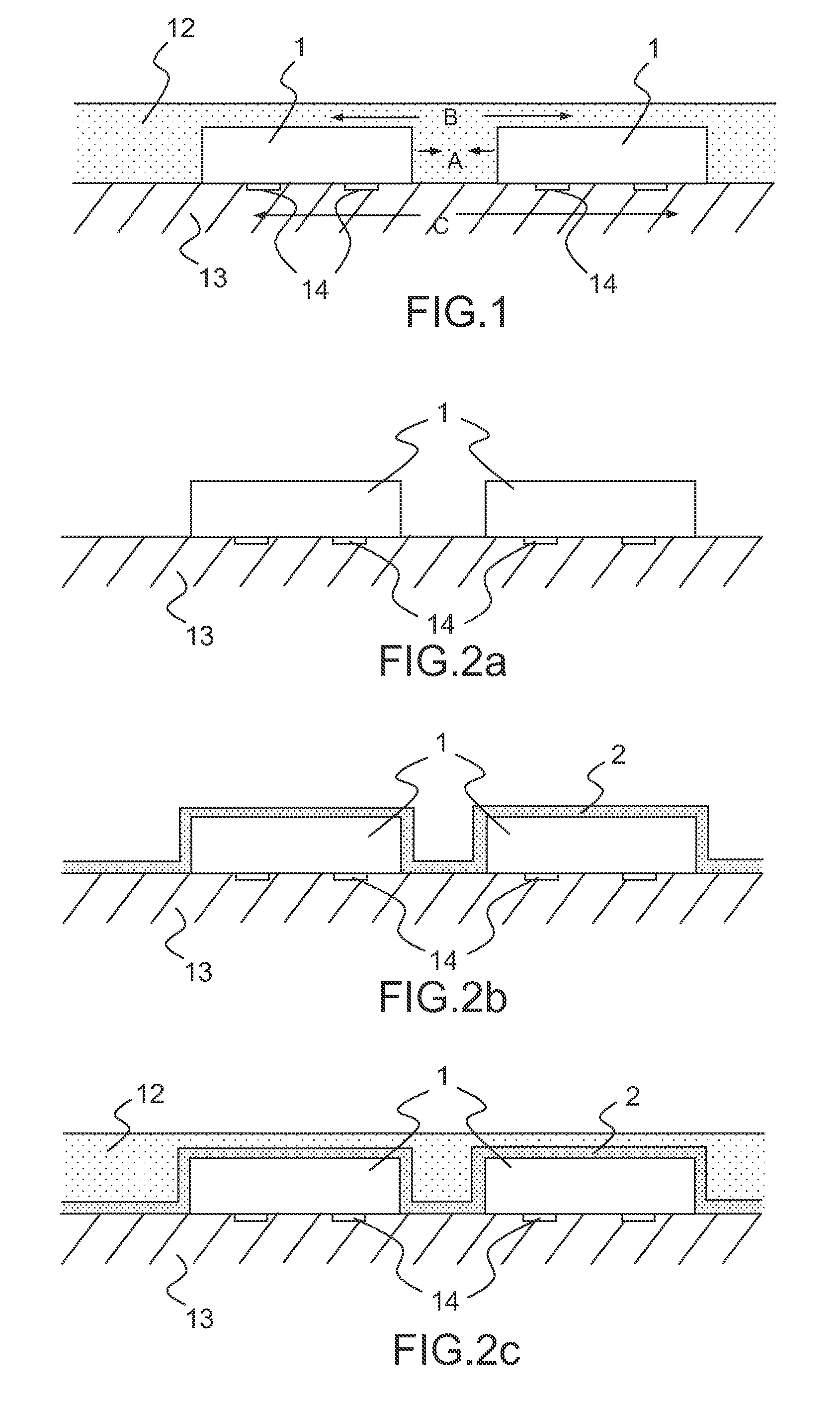
[0047]The holding of the chips after the “Pick and Place” placement step is obtained by a (or several) vapor deposition(s) at atmospheric pressure and at ambient temperature, of electrically insulating mineral materials, this deposition being able to remain throughout the entire method of fabrication or else be partially dissolved chemically as will be seen.

[0048]The main steps of the method are described in conjunction with FIG. 2.

[0049]In a conventional manner, the chips 1 are overlaid and positioned on an adhesive support 13 comprising a “tacky skin”, the front faces comprising the connection pads 14 (also termed active faces) being on this adhesive support (FIG. 2a).

[0050]According to the invention, an electrically insulating layer 2 of a few microns (from 1 μm to 10 μm) is deposited on the whole of the reconstituted wafer, that is to say on the chips 1 and the support 13, at ambient temperature and at atmospheric pressure (FIG. 2b).

[0051]According to a first mode of production,...


PUM

PropertyMeasurementUnit
temperatureaaaaaaaaaa
pressureaaaaaaaaaa
temperatureaaaaaaaaaa

Abstract

A method for collectively fabricating a reconstituted wafer comprising chips exhibiting connection pads on a front face of the chip, comprises: positioning the chips on an initial adhesive support, front face on the support, vapor deposition at atmospheric pressure and ambient temperature, of an electrically insulating layer on the initial support and the chips, having a mechanical role of holding the chips, transfer of the chips covered with the mineral layer onto a provisional adhesive support, rear face of the chips toward this provisional adhesive support, removal of the initial adhesive support, overlaying the chips onto a support of “chuck” type, front faces of the chips toward this support, removal of the provisional adhesive support, deposition of a resin on the support of “chuck” type to encapsulate the chips, and then polymerization of the resin, removal of the support of “chuck” type, production of an RDL layer active face side.

Description

CROSS-REFERENCE TO RELATED APPLICATIONS[0001]This application is a National Stage of International patent application PCT / EP2012 / 058195, filed on May 4, 2012, which claims priority to foreign French patent application No. FR 1153902, filed on May 6, 2011, the disclosures of which are incorporated by reference in their entirety.FIELD OF THE INVENTION[0002]The field of the invention is that of the fabrication of reconstituted wafers which comprise chips encapsulated in a resin, these chips having in general been tested beforehand.BACKGROUND[0003]The solution most commonly implemented to produce a reconstituted wafer consists firstly in slicing wafers on which chips have been fabricated to obtain individual chips, a wafer producing mutually identical chips of a first type, another wafer producing chips of another type, etc. The term chip refers to an active electronic component such as a bare chip or a passive component (capacitors, resistors, transformers or inductors, etc.) or a MEMS...

Claims


Application Information

Patent Timeline
Patent Type & Authority Patents(United States)
IPC IPC(8): H01G4/224H05K3/28H01L23/00H01L21/56B05D5/10B05D1/02H01L23/31H05K1/11H05K1/18C23C16/01C23C14/08C23C16/40
CPCH01G4/224H01L21/568H01L24/18H01L24/82H01L24/96H01L24/97H05K3/284B05D1/02B05D5/10C23C14/08C23C16/01C23C16/402H01L23/3121H01L2221/68368H01L2224/24227H01L2224/73267H01L2224/97H01L2924/01005H01L2924/01006H01L2924/01013H01L2924/01029H01L2924/01058H01L2924/01061H01L2924/01079H01L2924/1461H01L2924/15153H05K1/115H05K1/181H01L2924/00H01L2224/83H01L2224/82H01L2924/181H01L23/538H01L23/48H01L23/31H01L21/56
Inventor VAL, CHRISTIAN
Owner 3D PLUS
Features
  • R&D
  • Intellectual Property
  • Life Sciences
  • Materials
  • Tech Scout
  • Unparalleled Data Quality
  • Higher Quality Content
  • 60% Fewer Hallucinations
Learn More