Converter having partially thinned leadframe with stacked chips and interposer, free of wires and clips

a technology of leadframe and interposer, which is applied in the direction of semiconductor devices, solid-state devices, basic electric elements, etc., can solve the problems of significant parasitic inductance into the power circuit, parasitic system, and risk of wire sweep and subsequent electrical shorts, so as to reduce the board area consumed, reduce the height, and improve the effect of system performan

Active Publication Date: 2015-09-15
TEXAS INSTR INC
View PDF5 Cites 3 Cited by
  • Summary
  • Abstract
  • Description
  • Claims
  • Application Information

AI Technical Summary

Benefits of technology

[0007]For DC / DC power converters, the relentless market trend towards miniaturization calls for reduction of the board area consumed by the assembled system, as well as for reduced height. Needless to say that these goals should preferably be achieved while simultaneously the system performance is improved and the cost is reduced.
[0008]Applicant realized that the height of a system of chips and clips vertically assembled on a leadframe pad can be reduced when the low-side FET chip is embedded in the leadframe pad, which has a thinned out pocket to allow the insertion of a chip. After insertion, one terminal of the chip is electrically attached to the pad and the exposed other terminals of the chip become co-planar with the surface of the un-thinned pad portions and the leads.
[0009]Investigating ways of eliminating elements without sacrificing their functions, applicant discovered a method of drastically reducing the system height by replacing both clips with a single interposer and eliminating the discrete driver-and controller chip by integrating its circuitry into the chip of the high-side FET. The flat interposer is pre-fabricated by stamping and coining a metallic leadframe from a sheet of metal into a network of partially thinned low-resistance traces able to carry high currents and to spread heat, and then by filling the gaps and partially thinned metal portions with an insulating and re-enforcing molding compound. The interposer, stacked on the leadframe pad, has one trace attached to the terminals of the low-side chip inserted in the pad pocket, and other traces attached to the leads. Other interposer traces are attached to the high-side chip stacked on top of the interposer with the terminals of the high-side FET and the integrated driver-and-control circuitry. The stack of leadframe, interposer and chips may be encapsulated in a packaging compound; however, it is a technical advantage when the un-attached surface of the high-side chip is left un-encapsulated so that it is available for attaching a heat sink. This sink, together with the leadframe pad connected to a board sink, allows the double cooling of the system.

Problems solved by technology

The electrical connections from the chips to the leads may be provided by bonding wires, which introduce, due to their lengths and resistances, significant parasitic inductance into the power circuit.
Independent of the physical size, the sync FET chip needs a larger active area than the active area of the control FET chip, due to considerations of duty cycle and conduction loss.
Due to their forms and materials, the clips and wire bonds have resistances and inductances, which contribute to the parasitics of the system.
This assembly structure saves real estate of the leadframe pad and thus the printed circuit board, but accepts the risk of very long downhill bonding wires and thus the risk of wire sweep and subsequent electrical shorts during the encapsulation process.

Method used


Image

  • Converter having partially thinned leadframe with stacked chips and interposer, free of wires and clips
  • Converter having partially thinned leadframe with stacked chips and interposer, free of wires and clips
  • Converter having partially thinned leadframe with stacked chips and interposer, free of wires and clips

Examples


Embodiment Construction

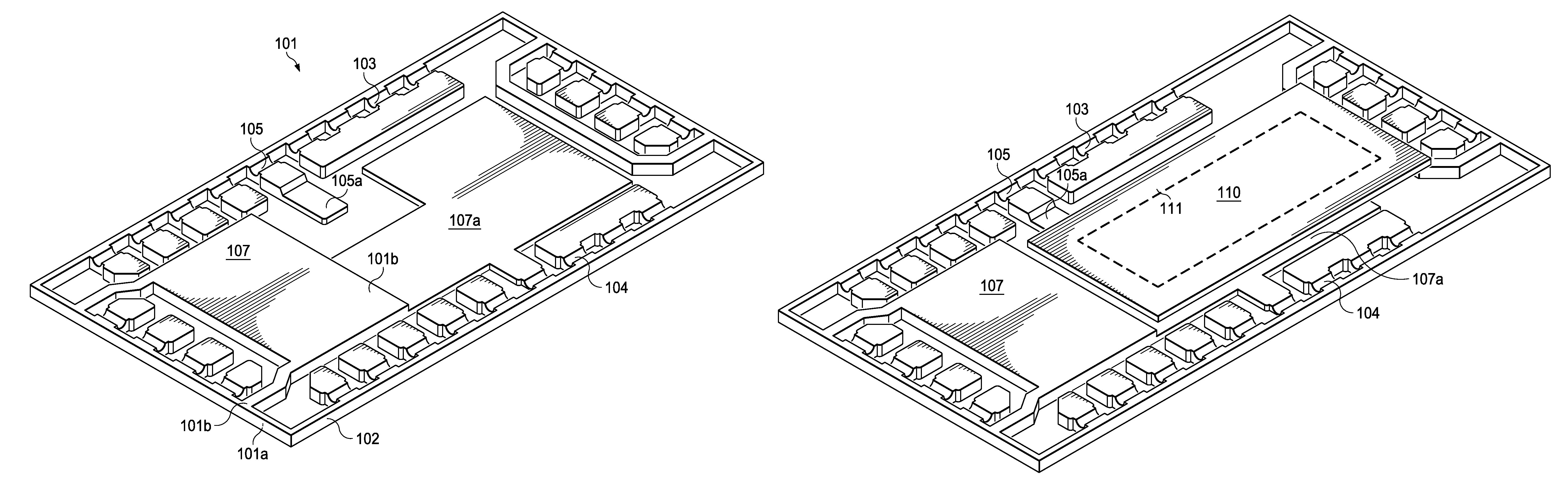
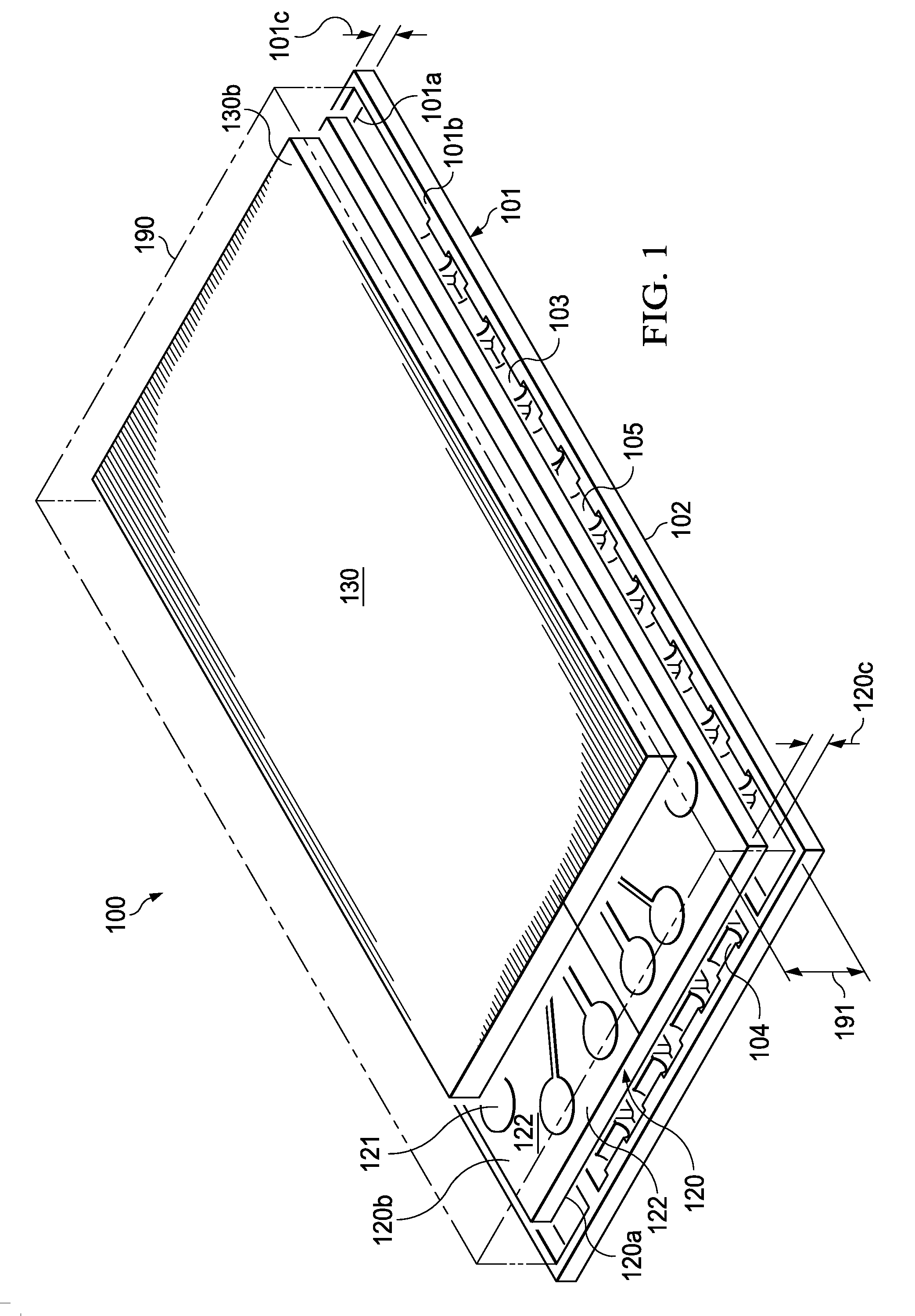
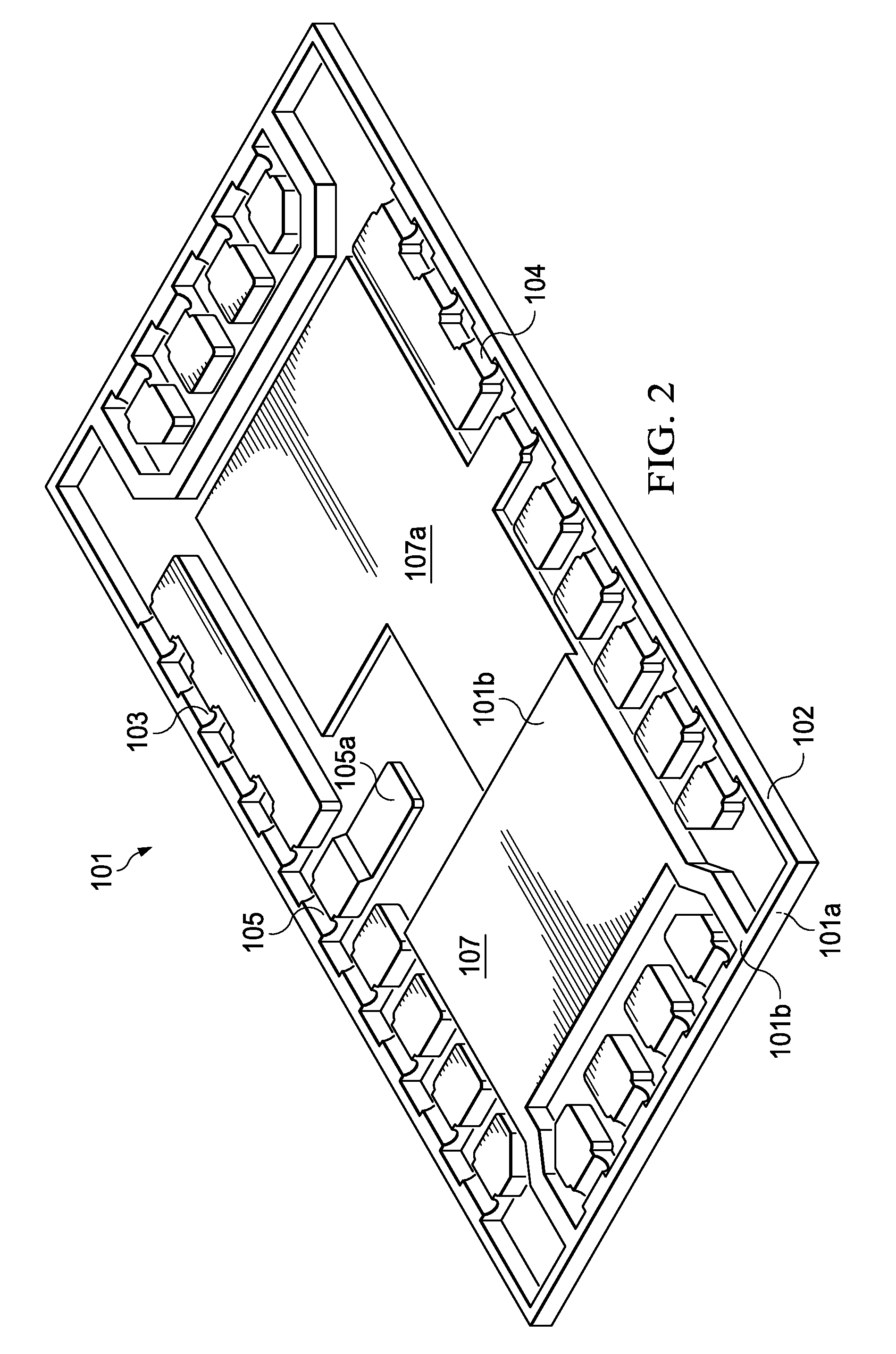
[0020]FIG. 1 illustrates a power supply system such as a DC / DC converter generally designated 100 as an exemplary embodiment of the invention; the system is shown before the step of trimming the rails 102 of the leadframe 101. For explanatory reasons, system 100 is shown with a transparent encapsulation 190. Preferred actual encapsulation uses a black-colored epoxy formulation suitable for a transfer molding technology. The exemplary system of FIG. 1 has a thickness 191 of 192 of about 5 mm and a width 193 of about 6 mm. Other systems may be square-shaped; some are as small as 3 mm by 3 mm.

[0021]Visible through the transparent encapsulation is a vertically assembled stack, which includes sequentially a leadframe 101, a first chip with FET terminals of opposite sides (not visible in FIG. 1), a flat interposer 120, and a second chip 130 with FET terminals on one side (this side not visible in FIG. 1). FIG. 1 shows the bare silicon surface of second chip 130. Metal leadframe 101 is gen...


PUM


Abstract

Power supply system (100) comprises vertically sequentially a QFN leadframe (101), a first chip (110) with FET terminals on opposite sides, a flat interposer (120), and a second chip (130) with FET terminals and the terminals of the integrated driver-and-control circuit on a single side. Leadframe pad (107) has a portion (107a) recessed as pocket with a depth and an outline suitable for attaching the first chip with one terminal in the pocket and the opposite terminal co-planar with the un-recessed pad surface. The interposer comprises metal patterned in traces separated by gaps; the traces include metal of a first height and metal of a second height smaller than the first height, and insulating material filling the gaps and the height differences; one interposer side attached to the leadframe pad with the first chip, the opposite interposer side attached to the terminals of the second chip.

Description

FIELD OF THE INVENTION[0001]The present invention is related in general to the field of semiconductor devices and processes, and more specifically to the structure and fabrication method of DC / DC converters, which have a partially thinned leadframe with stacked chips and an interposer, and are free of wires and clips.DESCRIPTION OF RELATED ART[0002]Among the popular families of power supply circuits are the power switching devices for converting on DC voltage to another DC voltage. Particularly suitable for the emerging power delivery requirements are the Power Blocks with two power MOS field effect transistors (FETs) connected in series and coupled together by a common switch node; such assembly is also called a half bridge. When a regulating driver and controller is added, the assembly is referred to as Power Stage or, more commonly, as Synchronous Buck Converter. In the synchronous Buck converter, the control FET chip, also called the high-side switch, is connected between the su...

Claims


Application Information

Patent Timeline
Patent Type & Authority Patents(United States)
IPC IPC(8): H01L21/44H01L23/495H01L23/498H01L21/56H02M7/00H01L25/00H01L25/16H01L23/31
CPCH01L25/165H01L21/56H01L23/3107H01L23/49503H01L23/49562H01L23/49568H01L23/49575H01L23/49838H01L25/50H02M7/003H01L23/49531H01L23/49548H01L23/49861H01L25/074H01L23/3114
Inventor JOSHI, RAJEEV DINKAR
Owner TEXAS INSTR INC
Why Eureka
Try Eureka