On-chip power-combining for high-power schottky diode based frequency multipliers

a technology of schottky diodes and power combining, which is applied in the direction of diodes, oscillator generators, semiconductor/solid-state device details, etc., can solve the problems of increasing the electrical path of the signal, using traditional power-combining topologies, and inconvenience beyond 1 thz

Active Publication Date: 2015-09-22
CALIFORNIA INST OF TECH
View PDF6 Cites 197 Cited by
  • Summary
  • Abstract
  • Description
  • Claims
  • Application Information

AI Technical Summary

Benefits of technology

[0014]The frequency of the input signal can be W-band or higher, i.e. within the terahertz range (100 GHz-3 THz). The output frequency can be twice or three times the input signal depending on the multiplier type. The MMIC multiplier device features one antenna (E-probe) per multiplying structure. The 2 or more antennas of the whole chip are symmetrically placed within the plane normal to the propagation of the incident electrical field (TE10 mode of the input waveguide). The 2 or more antennas thereby split evenly the incident power among the 2 or more multiplying structures included on the same MMIC chip.

Problems solved by technology

However, the use of traditional power-combining topologies, already demonstrated below 1 THz, presents inconvenience beyond 1 THz.
On the one hand, the use of Y-junction to divide / combine the input / output power at these frequency bands unnecessarily increases the electrical path of the signal at a range of frequencies where waveguide losses are considerably high.
On the other hand, guaranteeing a perfect alignment of the very small chips during assembly, in order to preserve the balanced nature of the multiplier, is practically impossible, with a subsequent impact on the multiplier performance.

Method used


Image

  • On-chip power-combining for high-power schottky diode based frequency multipliers
  • On-chip power-combining for high-power schottky diode based frequency multipliers
  • On-chip power-combining for high-power schottky diode based frequency multipliers

Examples


Embodiment Construction

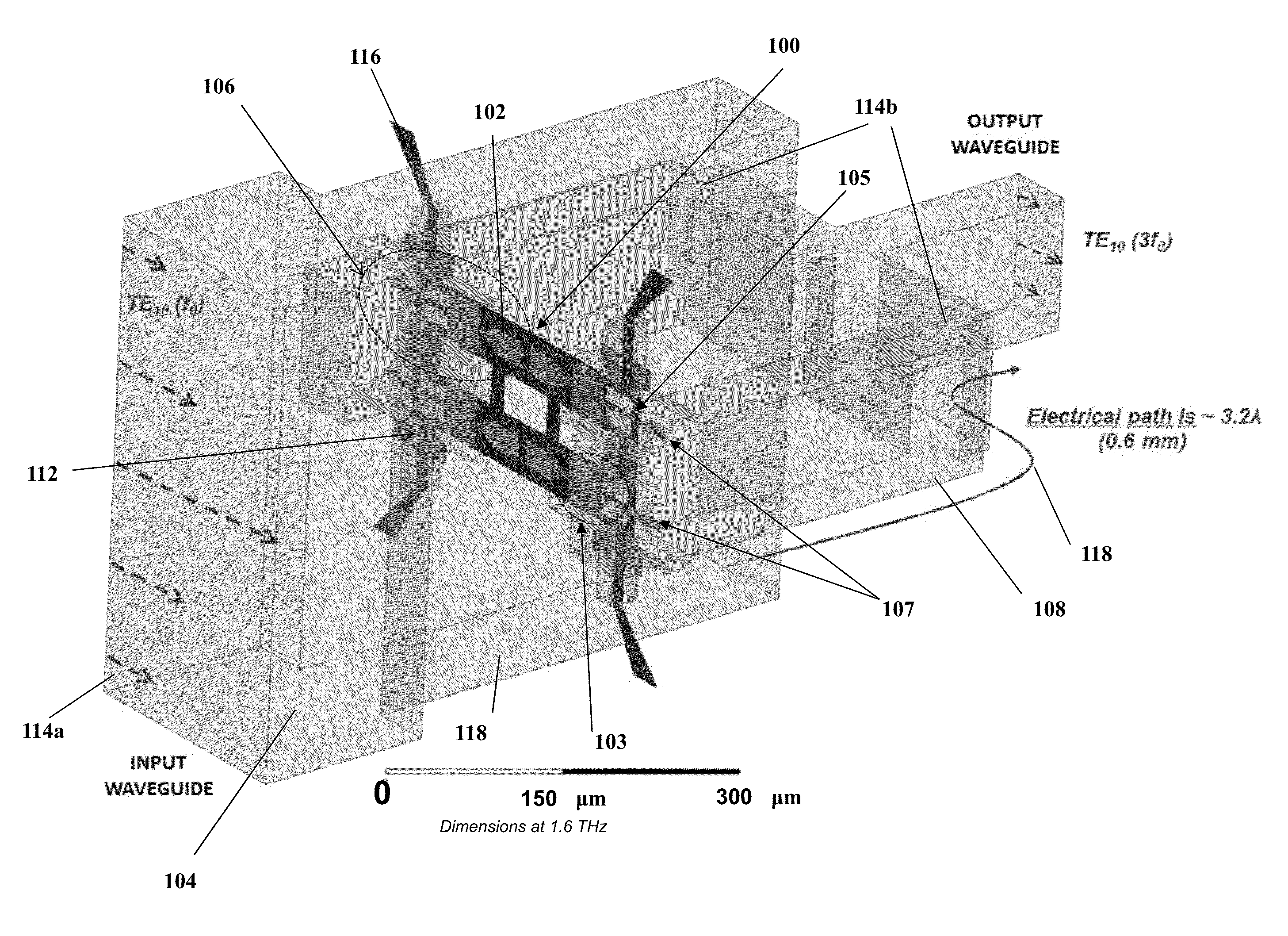
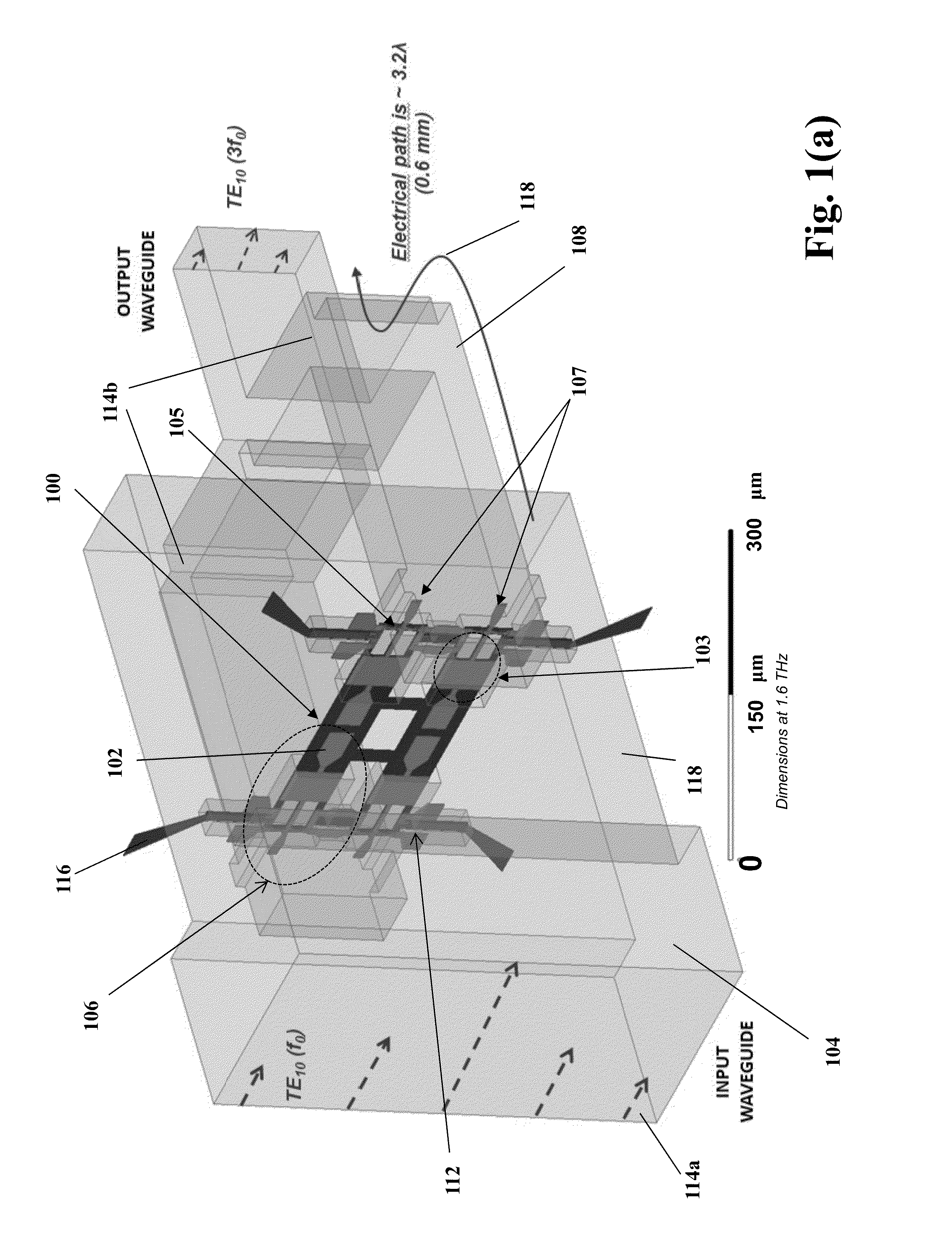
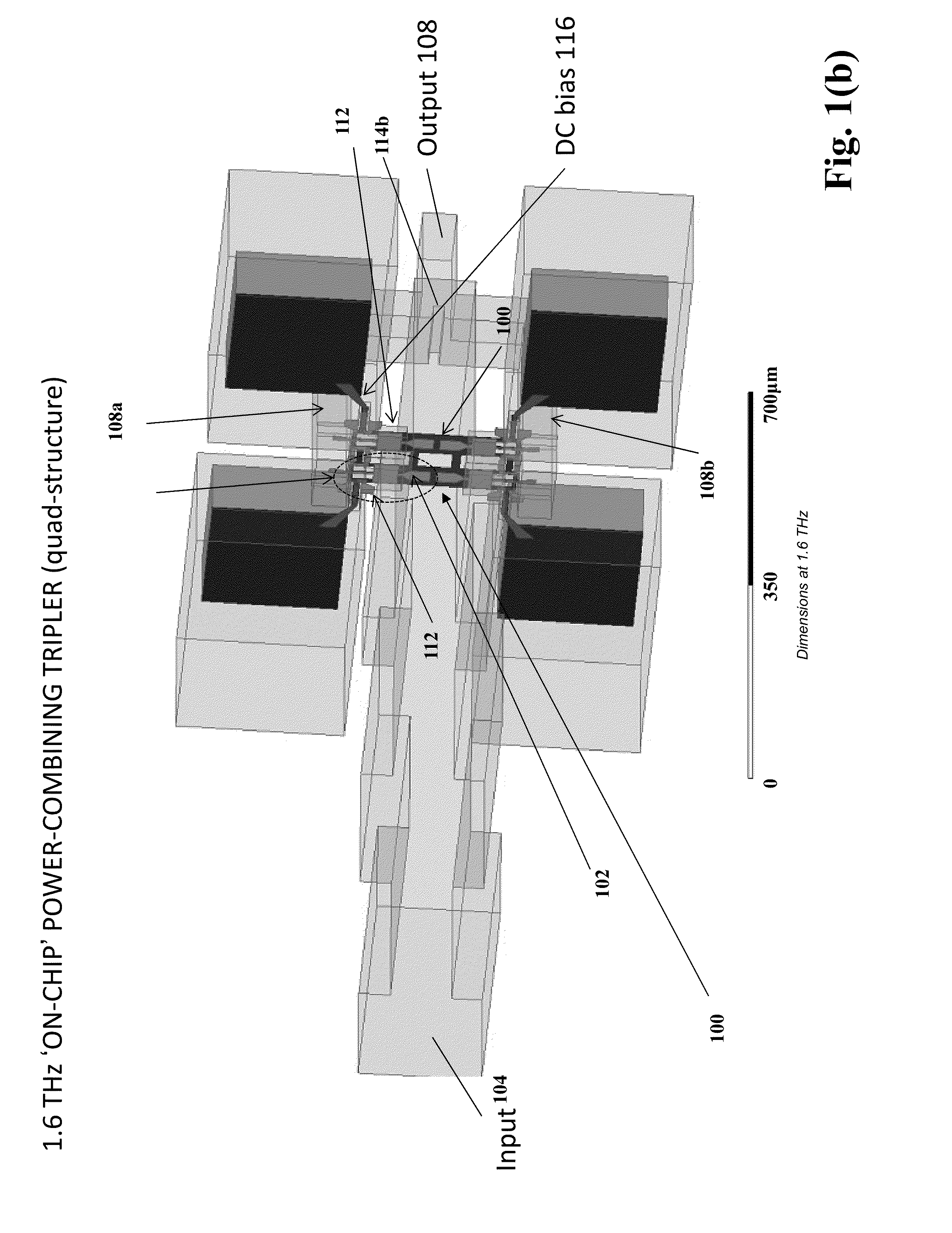
[0053]In the following description of the preferred embodiment, reference is made to the accompanying drawings which form a part hereof, and in which is shown by way of illustration a specific embodiment in which the invention may be practiced. It is to be understood that other embodiments may be utilized and structural changes may be made without departing from the scope of the present invention.

[0054]In spite of the fact that some specific circuit designs at certain operation frequencies within the submillimeter-wave and terahertz ranges are used as reference to describe the invention, the described topology is applicable to any frequency range, input power levels, number of diodes and bias condition. All these different conditions shall be covered with the present patent application.

[0055]Technical Description

[0056]One or more embodiments of the present invention disclose a novel power-combined Schottky frequency multiplier topology intended to increase by a number of 2 or more t...


PUM


Abstract

A novel MMIC on-chip power-combined frequency multiplier device and a method of fabricating the same, comprising two or more multiplying structures integrated on a single chip, wherein each of the integrated multiplying structures are electrically identical and each of the multiplying structures include one input antenna (E-probe) for receiving an input signal in the millimeter-wave, submillimeter-wave or terahertz frequency range inputted on the chip, a stripline based input matching network electrically connecting the input antennas to two or more Schottky diodes in a balanced configuration, two or more Schottky diodes that are used as nonlinear semiconductor devices to generate harmonics out of the input signal and produce the multiplied output signal, stripline based output matching networks for transmitting the output signal from the Schottky diodes to an output antenna, and an output antenna (E-probe) for transmitting the output signal off the chip into the output waveguide transmission line.

Description

CROSS REFERENCE TO RELATED APPLICATIONS[0001]This application claims the benefit under 35 U.S.C. Section 119(e) of the following co-pending and commonly-assigned application:[0002]U.S. Provisional Patent Application Ser. No. 61 / 527,506, filed on Aug. 25, 2011, by Goutam Chattopadhyay, Imran Mehdi, Erich T. Schlecht, Choonsup Lee, Jose V. Siles, Alain E. Maestrini, Bertrand C. Thomas, Cecile D. Jung, entitled “ON-CHIP POWER-COMBINING FOR HIGH-POWER SCHOTTKY DIODE BASED FREQUENCY MULTIPLIERS,” which application is incorporated by reference herein.STATEMENT REGARDING FEDERALLY SPONSORED RESEARCH AND DEVELOPMENT[0003]The invention described herein was made in the performance of work under a NASA contract, and is subject to the provisions of Public Law 96-517 (35 USC 202) in which the Contractor has elected to retain title.BACKGROUND OF THE INVENTION[0004]1. Field of the Invention[0005]This invention relates to on-chip power combining for high-power Schottky diode based frequency multipl...

Claims


Application Information

Patent Timeline
Patent Type & Authority Patents(United States)
IPC IPC(8): H03B19/16H03B19/18H01L21/77H01L27/08H01L23/66
CPCH03B19/16H01L21/77H03B19/18H01L23/66H01L27/0814H01L2223/6627H01L2223/6677H01L2223/6683H01L2224/48091H01L2924/12032H03B2200/0032H03B2200/0076H01L2924/00014H01L2924/00
Inventor SILES PEREZ, JOSE VICENTECHATTOPADHYAY, GOUTAMLEE, CHOONSUPSCHLECHT, ERICH T.JUNG-KUBIAK, CECILE D.MEHDI, IMRAN
Owner CALIFORNIA INST OF TECH
Why Eureka
Try Eureka