Making imprinted micro-wire rib structure

a micro-wire and rib structure technology, applied in the field of imprinted structures, can solve the problems of increasing the cost of deposited and pattern, increasing the cost of transparent conductive metal oxides, and increasing the cost of material requirements, so as to reduce the need for materials, increase manufacturing speed and simplicity, and reduce the effect of space requirements

Active Publication Date: 2015-10-13
EASTMAN KODAK CO
View PDF10 Cites 11 Cited by
  • Summary
  • Abstract
  • Description
  • Claims
  • Application Information

AI Technical Summary

Benefits of technology

[0018]Structures and methods of the present invention provide larger and more conductive micro-wires using less space than alternative structures and meth

Problems solved by technology

Transparent conductive metal oxides are well known in the display and touch-screen industries and have a number of disadvantages, including limited transparency and conductivity and a tendency to crack under mechanical or environmental stress.
Transparent conductive metal oxides are increasingly expensive and relatively costly to deposit and pattern.
Moreover, the substrate materials are limited by the electrode material deposition process (e.g. sputtering) and the current-carrying capacity of such electrodes is limited, thereby limiting the amount of power that can be supplied to the pixel elements.
Although thicker layers of metal oxides or metals increase conductivity, they also reduce the transparency of the electrodes.
However, in other portions of a substrate, for example in a bezel area around the periphery of a substrate associated with display,

Method used


Image

  • Making imprinted micro-wire rib structure
  • Making imprinted micro-wire rib structure
  • Making imprinted micro-wire rib structure

Examples


Embodiment Construction

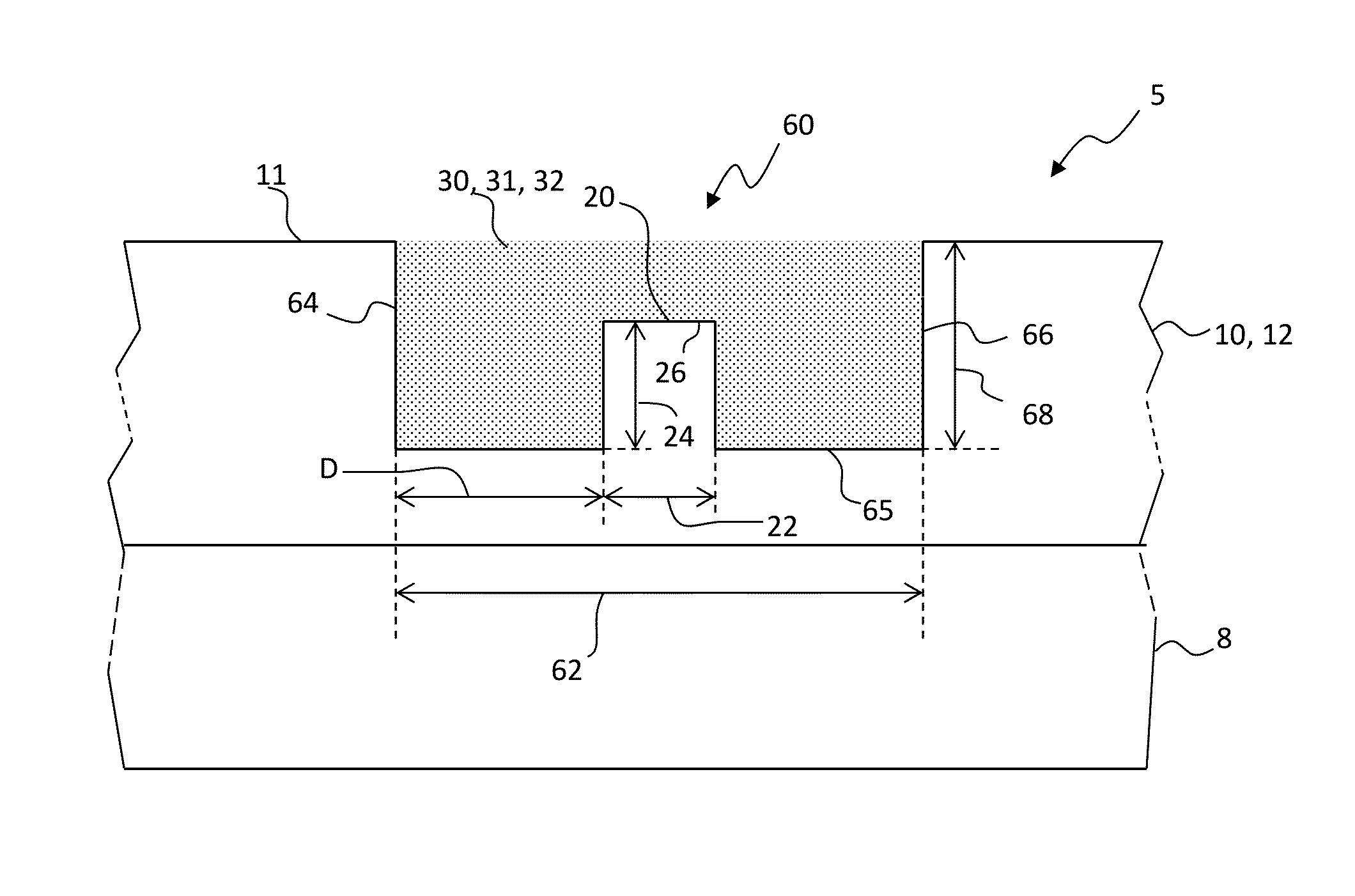
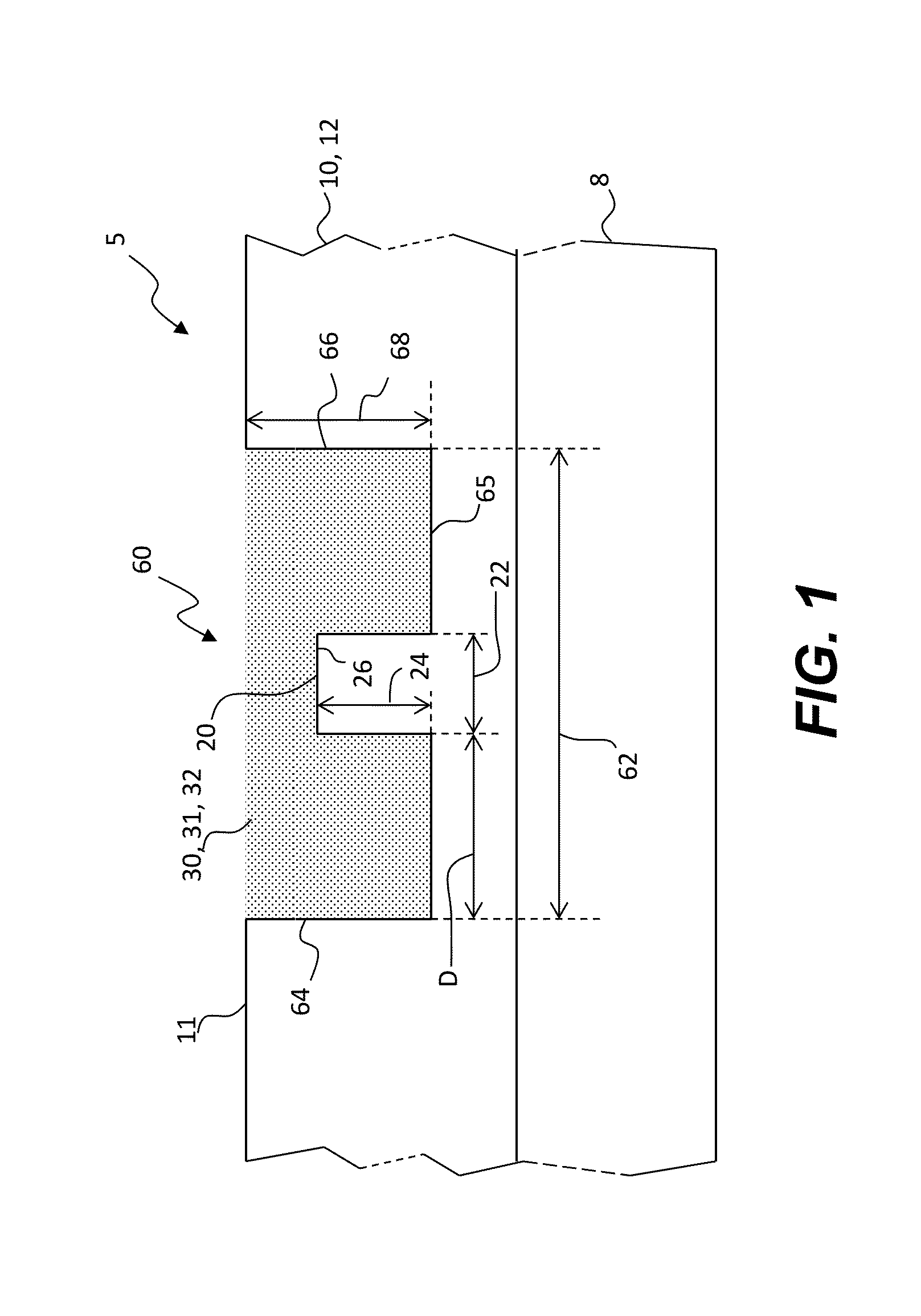
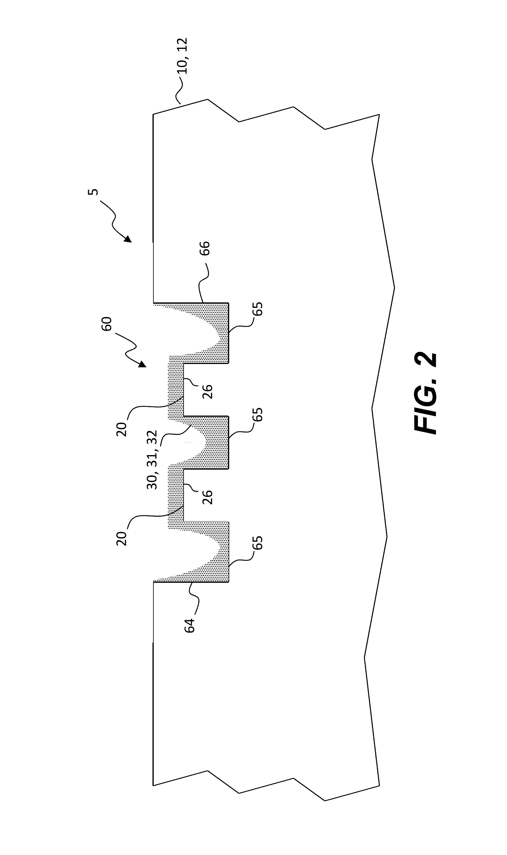
[0028]Substrates used in combination with displays, for example touch screens, typically have a display area in which transparency is important and a peripheral area used to connect electrodes in the display area to external or local electrical components in the peripheral area using electrical buses. For example, capacitive touch screens use spaced-apart electrically connected micro-wires to form electrodes in the display area. However, such micro-wires are limited in their current-carrying capacity so that they are not suitable as high-conductivity electrical buses for connecting connection pads or electrical components in the peripheral area to the electrodes in the display area. Either multiple such micro-wires are used, requiring additional substrate space in the peripheral area, or alternative conductive materials or processes must be used, requiring additional manufacturing steps and increasing costs. It is desirable to limit the size of the peripheral area to increase the di...


PUM


Abstract

A method of making a micro-wire rib structure includes providing a substrate and locating a curable layer on or over the substrate. The curable layer is imprinted and cured to form a cured layer including a cured-layer surface and a micro-channel having a micro-channel depth, a micro-channel bottom, first and second micro-channel sides, and one or more ribs having opposing rib sides and a rib top defining a rib height less than the micro-channel depth. Each rib is located between the first and second micro-channel sides and extends from the micro-channel bottom toward the cured-layer surface. A curable conductive material is located in the micro-channel and cured to provide a cured electrical conductor forming a micro-wire in the micro-channel. The micro-wire extends continuously from the first micro-channel side, over the micro-channel bottom, the rib side(s) and rib top(s), to the second micro-channel side forming a continuous electrical conductor from the first micro-channel side to the second micro-channel side.

Description

CROSS REFERENCE TO RELATED APPLICATIONS[0001]Reference is made to commonly-assigned U.S. patent application Ser. No. 14 / 476,005 filed Sep. 3, 2014, entitled IMPRINTED MICRO-WIRE RIB STRUCTURE by Cok; to commonly-assigned U.S. patent application Ser. No. 14 / 475,896 entitled RIBBED LARGE-FORMAT IMPRINTED METHOD by Cok; to commonly-assigned U.S. patent application Ser. No. 13 / 784,866 (now published as U.S. 2014 / 02516601 entitled VARIABLE DEPTH MICRO-CHANNEL STRUCTURE by Cok; and to commonly-assigned U.S. Pat. No. 8,895,429 entitled MICRO-CHANNEL STRUCTURE WITH VARIABLE DEPTHS by Cok; the disclosures of which are incorporated herein.FIELD OF THE INVENTION[0002]The present invention relates to imprinted structures having micro-channels filled with cured electrically conductive materials.BACKGROUND OF THE INVENTION[0003]Transparent conductors are widely used in the flat-panel display industry to form electrodes that are used to electrically switch light-emitting or light-transmitting prop...

Claims


Application Information

Patent Timeline
IPC IPC(8): H01L21/4763H05K3/00H05K3/12
CPCH05K3/1258H05K3/125H05K3/0014H05K3/1283H05K2203/06H05K2201/0108H05K2203/0108H05K2203/088
Inventor COK, RONALD STEVENBURBERRY, MITCHELL STEWART
Owner EASTMAN KODAK CO
Why Eureka
Try Eureka