Display device and electoric device having the same

a display device and electoric device technology, applied in static indicating devices, instruments, electroluminescent light sources, etc., can solve the problems of high speed of a signal line driver circuit, affecting the current flow through the light-emitting element, uneven display and display quality degradation, etc., to achieve the effect of reducing the total circuit area, reducing the power consumption and ensuring the length of the writing period

Inactive Publication Date: 2015-10-20
SEMICON ENERGY LAB CO LTD
View PDF21 Cites 3 Cited by
  • Summary
  • Abstract
  • Description
  • Claims
  • Application Information

AI Technical Summary

Benefits of technology

[0039]In a time division gradation method (also referred to as a time gray-scale method) which is one of the driving methods of a display device, a row writing period is divided into half, the first half of the row writing period (a first row writing period) is used for writing video signals (also referred to as a video signal) into pixels, and the second half of the row writing period (a second row writing period) is used for writing signals into each pixel for forcibly stopping current supply to a light-emitting element. By writing such signals for forcibly stopping current supply to a light-emitting element into each pixel, a non-display period is provided; thus, the sub-frame period can be made shorter than the writing period. With the use of the scanning line driver circuit having the structure of the present invention, there is no need to repeat charge and discharge of all scanning lines in an erasing period which is a period where signals for forcibly stopping current supply to light-emitting elements are input; therefore, the power consumption can be reduced considerably. Moreover, with the use of the scanning line driver circuit having the structure of the present invention, there is no need to provide a switching circuit or the like. Further, with the use of the scanning line driver circuit having the structure of the present invention, the scanning line driver circuit can be operated by being arranged only on one side; therefore, the total circuit area can be reduced considerably.
[0040]Additionally, the length of the writing period can be secured even when the number of sub-frame appearing in one frame period is increased; therefore, the number of gray scales can be increased while suppressing the drive frequency of a driver circuit. In addition, even when the sub-frame is further divided into a plurality of sub-frame, the length of the writing period can be secured; therefore, the generation of pseudo contours can be suppressed while suppressing the drive frequency of a driver circuit.
[0041]Moreover, by using the scanning line driver circuit, without limitation to the erasing period, it is possible to select different scanning lines in one scanning line selection period and to input a different video signal to each scanning line. Therefore, light emission of a light-emitting element can be performed in sub-frame periods without provision of an erasing period. Accordingly, display can be performed without decrease of a duty ratio; thus, low power consumption can be realized and a wiring width can also be narrowed.

Problems solved by technology

However, when there is variation of characteristics of the driving transistor in each pixel due to a manufacturing process of the transistor or the like, the amount of current flowing through the light-emitting element is affected.
In particular, when effective Vgs (hereinafter, referred to as eVgs) is non-uniform depending on pixels due to the variation of threshold voltage (hereinafter, referred to as Vth) of the transistor, emission luminance differs widely among pixels, which results in display unevenness and deterioration of display quality.
In addition, in the digital time gray-scale method, there are problems such as high speed of a signal line driver circuit, increase of a video signal in division number, and increase in number of transistors of each pixel.

Method used


Image

  • Display device and electoric device having the same
  • Display device and electoric device having the same
  • Display device and electoric device having the same

Examples


embodiment 1

[Embodiment 1]

[0078]This embodiment will explain in detail the structure of a pixel of the display device described in Embodiment Mode.

[0079]The structure of the display device will be explained with reference to FIGS. 3A and 3B,

[0080]FIG. 4, and FIG. 5. A pixel 1010 includes a light-emitting element 1013, a capacitor element 1016, and two transistors. One of the two transistors is a switching transistor 1011 (hereinafter, also referred to as a TFT 1011) for controlling a video signal input to the pixel 1010, and the other is a driving transistor 1012 (hereinafter, also referred to as a TFT 1012) for controlling lighting and non-lighting of the light-emitting element 1013. Each of the TFTs 1011 and 1012 is a field effect transistor, which includes three terminals, a gate electrode, a source electrode, and a drain electrode.

[0081]A gate electrode of the TFT 1011 is connected to a gate line Gy, one of a source electrode and a drain electrode thereof is connected to a source line Sx, a...

embodiment 2

[Embodiment 2]

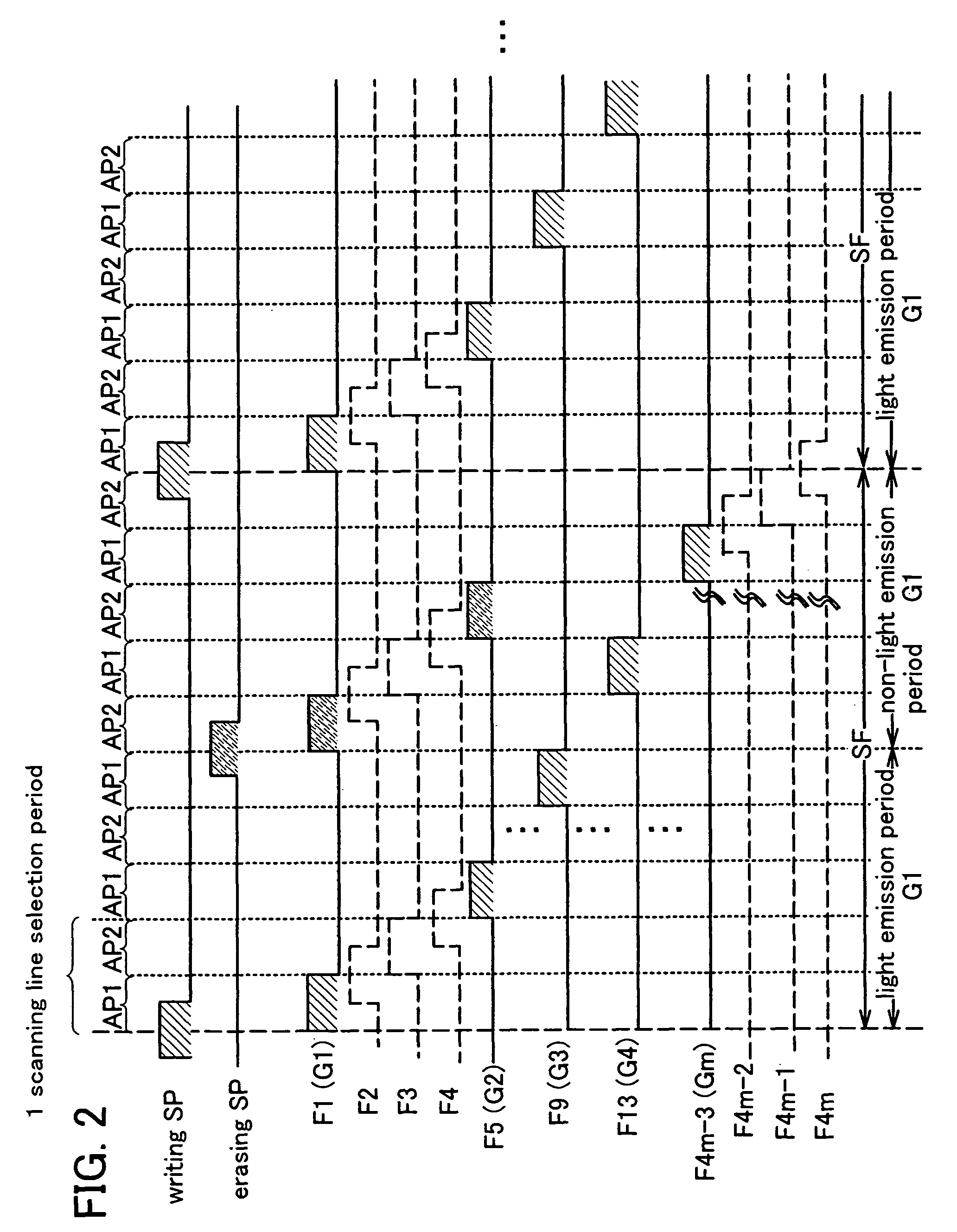
[0097]This embodiment will explain the operation of a display device having the pixels described in Embodiment 1 with reference to a timing chart (FIG. 6A) whose vertical axis denotes a scanning line while horizontal axis denotes time, and a timing chart (FIG. 6B) of a gate line Gi (1≦i≦m) in an i-th row. In a time gray-scale method, one frame period includes a plurality of sub-frame periods SF1, SF2, . . . , and SFn (n is a natural number).

[0098]Each of the plurality of sub-frame periods includes one of a plurality of writing periods Ta1, Ta2, . . . , and Tan in which the writing operation or the erasing operation is performed, and one of a plurality of light emitting elements Ts1, Ts2, . . . , and Tsn. Each of the plurality of writing periods includes a plurality of gate selection periods. Each of the plurality of gate selection periods includes a plurality of sub-gate selection periods. The number into which each gate selection period is divided is not particularly ...

embodiment 3

[Embodiment 3]

[0103]This embodiment will explain the operation different from that of the display device described in Embodiment 2.

[0104]The timing of each sub-frame period in this embodiment will be explained. FIG. 7A shows the timing of writing periods indicated by GAP1 at which video signals are written by a scanning line driver circuit in the first half period AP1 of one scanning line selection period which is explained in the above embodiment mode. In addition, the timing of writing periods indicated by GAP2 at which video signals are written by the scanning line driver circuit in the second half period AP2 of one scanning line selection period which is explained in the above embodiment mode is shown. Further, besides, the timing of each sub-frame period which appears in the pixels in the first row is shown. Note that FIG. 7A shows an example, where 8-bit video signals are used in a QVGA panel (320×240 pixels), for the explanation.

[0105]W1 to W8 each indicates the writing perio...


PUM


Abstract

It is an object of the present invention to provide a display device where power consumption can be suppressed and the number of gray scales can be increased without a scanning line driver circuit on both sides of a pixel portion. In a display device having a scanning line driver circuit, a shift register included in the scanning line driver circuit has 4m-stage (m is a natural number) flip-flop circuits in every m scanning lines, and a signal which selects the scanning line in a first half period of one scanning line selection period and a signal which selects the scanning line in a second half period of the one scanning line selection period are output to the scanning line by another start pulse.

Description

BACKGROUND OF THE INVENTION[0001]1. Field of the Invention[0002]The present invention relates to a display device. In particular, the present invention relates to the structure of a scanning line driver circuit in an active matrix display which includes a light-emitting element and which is manufactured by using a semiconductor device.[0003]A semiconductor device herein described indicates any device which can function by using a semiconductor characteristic.[0004]2. Description of the Related Art[0005]In recent years, demand for thin displays mainly applied to TVs, PC monitors, mobile terminals, or the like has increased rapidly, and further development has been promoted. The thin displays include a liquid crystal display device (LCD) and a display device equipped with a light-emitting element. In particular, an active matrix display using a self-light-emitting element is expected as a next-generation display for its features of high response speed, wide viewing angle, and capabili...

Claims


Application Information

Patent Timeline
Patent Type & Authority Patents(United States)
IPC IPC(8): G09G3/32G09G3/20G11C19/00H05B44/00
CPCG09G3/3266G09G3/20G11C19/00G09G3/2022G09G2310/0216G09G2310/0262G09G2310/0267G09G2320/029G09G2320/041G09G2320/043G09G2330/021
Inventor MIYAZAKI, AYA
Owner SEMICON ENERGY LAB CO LTD
Why Eureka
Try Eureka