Suppression of direct detection events in X-ray detectors

a detector and x-ray technology, applied in the field of detectors, can solve the problems of not all x-ray quanta are absorbed in the conversion layer, and substantially disturb the intended imag

Active Publication Date: 2015-12-01
KONINK PHILIPS ELECTRONICS NV
View PDF14 Cites 2 Cited by
  • Summary
  • Abstract
  • Description
  • Claims
  • Application Information

AI Technical Summary

Benefits of technology

[0014]Preferably the arbitration arrangement is designed for suppressing a radiation collection device output signal of a radiation collection device, which radiation collection device output signal's brightness differs by more than a predetermined value or factor from the brightness of radiation collection devices output signals of a plurality of further radiation collection devices. Such predetermined value or factor can have a very broad range of values depending on e.g. the detector apparatus. The predetermined value or factor can be chosen depending on the detector apparatus in a way which provides a satisfactory suppression of bright or dark direct detection event pixels without deteriorating the received image more than acceptable—the choice of the predetermined value or factor can theoretically also be done depending on a developers impression of received images if no other more convincing criteria would be found.

Problems solved by technology

A common problem with semiconductor X-ray detectors is that not all X-ray quanta are absorbed in the conversion layer, i.e. in the scintillator or photoconductor.
The number and position of bright pixels change from image to image and substantially disturb the intended image.

Method used


Image

  • Suppression of direct detection events in X-ray detectors
  • Suppression of direct detection events in X-ray detectors
  • Suppression of direct detection events in X-ray detectors

Examples


first embodiment

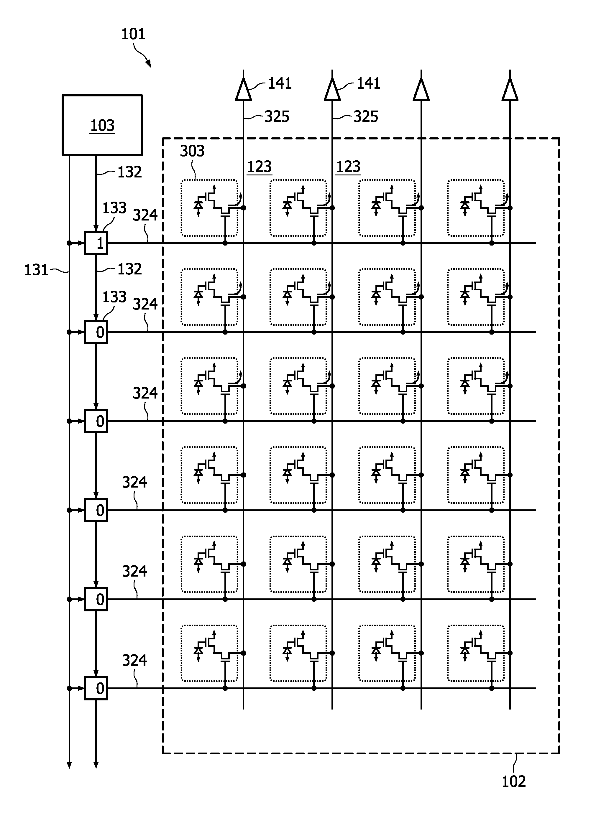
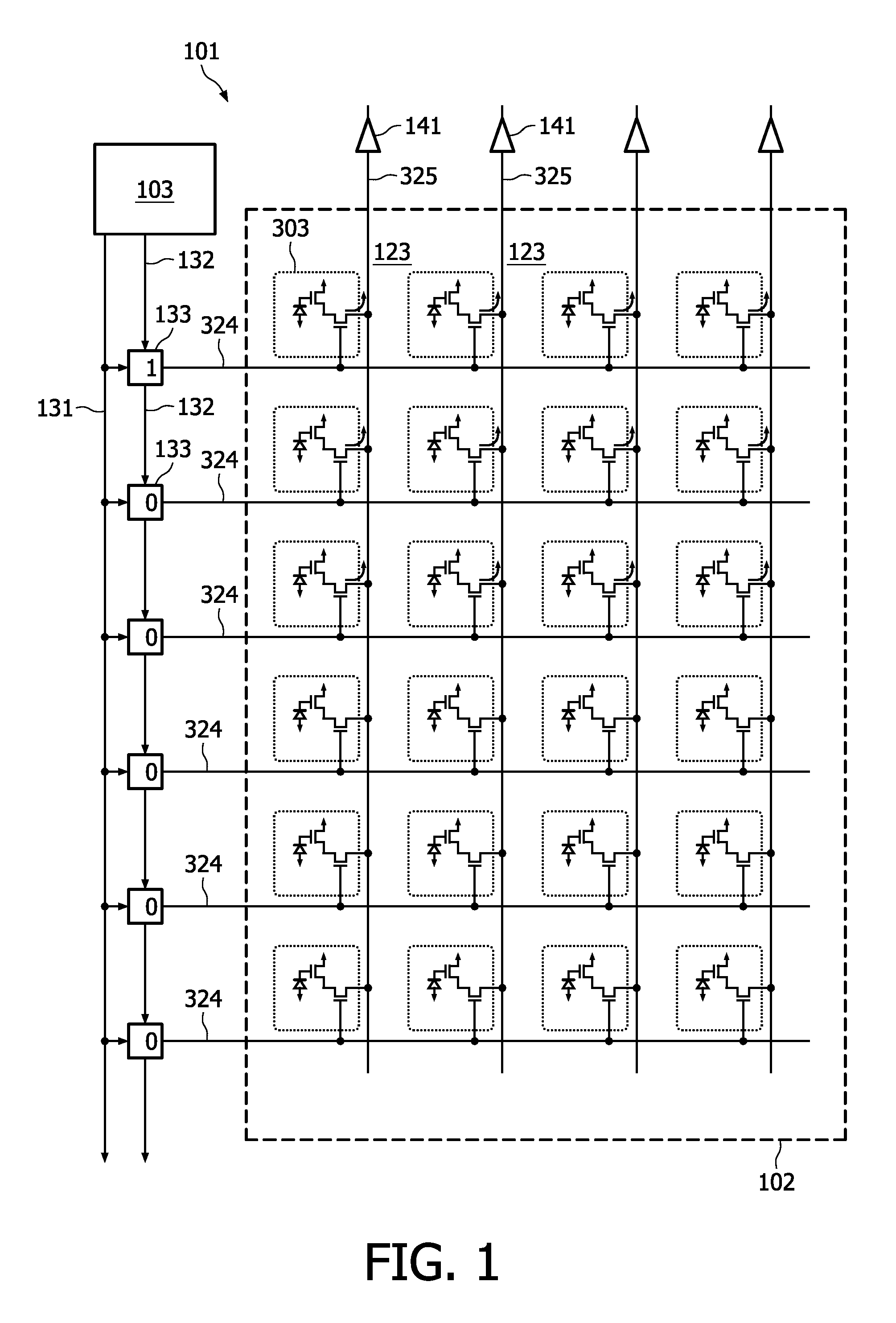
[0045] of the invention, e.g. two adjacent select lines (324) are activated at the same time and pairs of adjacent readout columns (325, 325) are connected by switches (142) between them. The further switches (142) are inactive. In this way, sets of four pixels are readout over the same column amplifiers (141) and the source terminals of the amplifier transistors are connected during readout. (Generally for arbitration according to the invention at least two pixels can be considered, preferably at least four are considered. A rectangular selection (e.g. all in 2 adjacent rows and all in 3 adjacent columns), of at least 1*2=2 pixels can be considered or a quadratic selection (e.g. all in 2 adjacent rows and all in (as many, i.e.) 2 adjacent columns) of at least 2*2=4 pixels can be considered.) In a normal image, all four pixels will have very similar brightness values. This leads to similar voltages on the photodiodes, resulting in similar gate source voltages in the four pixels and ...

second embodiment

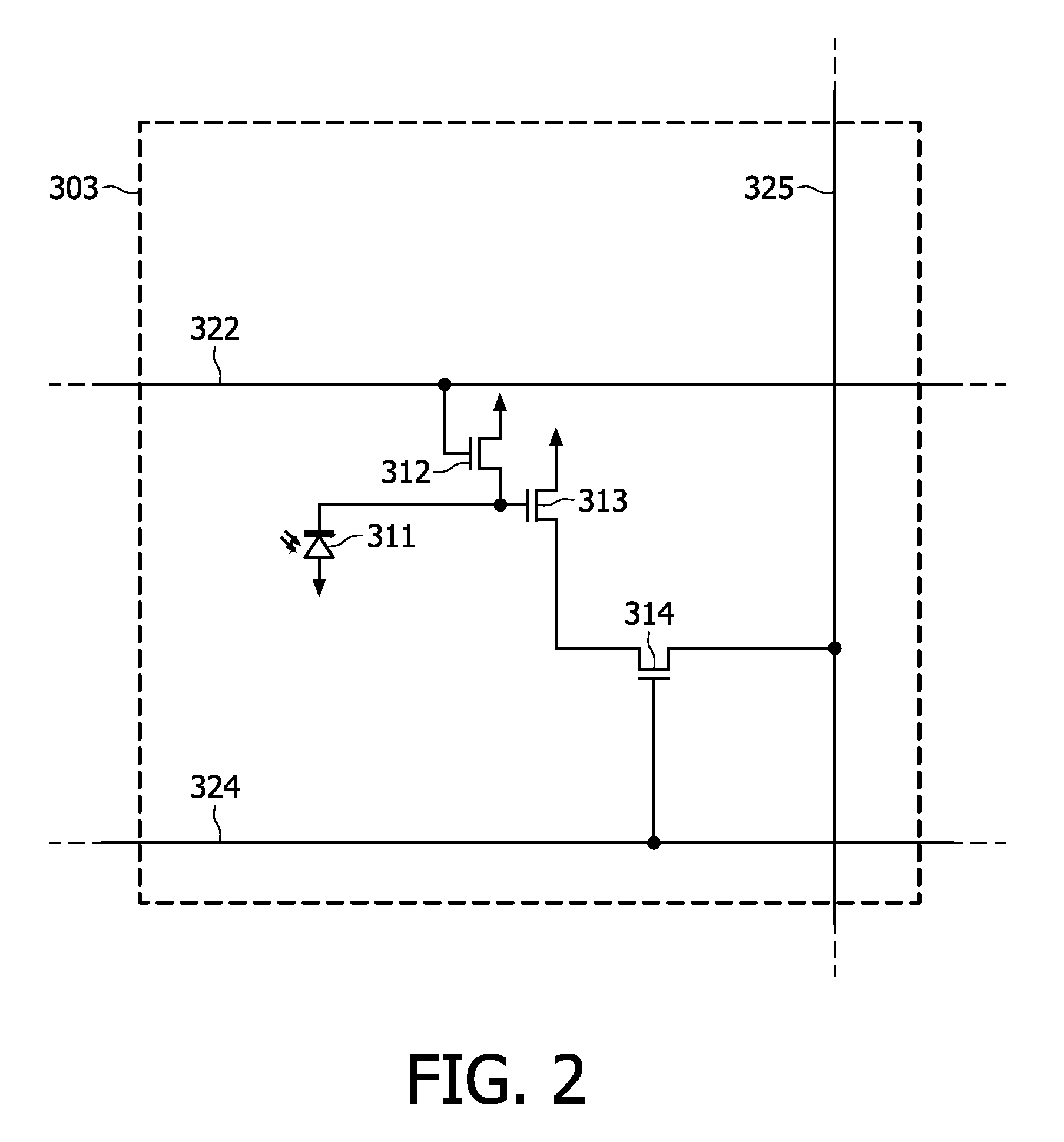
[0047]the invention uses a more sophisticated pixel cell depicted in FIG. 4. This cell (303) contains also a photodiode (311), a reset switch (312), an amplifier transistor (313), a readout switch (314) and the associated control and readout lines (322), (324), (325).

[0048]In addition, it has a sample and hold circuit consisting of sample switch (315), sample capacitor (316) and buffer amplifier (317). Following the X-ray exposure, the signal from the photodiodes can be transferred to the sample capacitor (316) by activating the sample switches (315). The sampled signal can be read out via the buffer (317) and readout switch (314) independently from the next exposure on the photodiode (311). The sampling action is often referred to a synchronous shutter in the imager world.

[0049]Additional switches (352) and lines (351) allow connecting the sampling capacitors in horizontal direction under control of a not shown control circuit. Likewise, additional switches (353) and columns (354) ...

third embodiment

[0053]the invention is depicted in FIG. 6. Here a pixel (303) is subdivided into four sub-pixels each comprising a photodiode (311), an amplifier transistor (313) and a sample switch (315). A number of radiation collection devices, e.g. photodiodes (311) and amplifier transistors (313) connect via sample switches (315) to a common sample capacitor (316). A buffer (317) and readout switch (314) allow readout of the pixel.

[0054]Analogically to the previous embodiments, a sub-pixel affected by a parasitic direct detection event will have a lower gate potential than the other pixels, hence it will contribute less to the charging of the sample capacitor. Consequently, the signal from the parasitic direct detection event will be effectively suppressed.

[0055]A modification of this circuit uses only one sampling switch (315). Its left terminal is directly connected to the source terminals of all amplifier transistors in the pixel (no figure).


PUM


Abstract

According to an embodiment of the invention, signals coming from a number of pixels or sub-pixels are compared and those signals from pixels or sub-pixels, which are substantially brighter than the other pixels in the comparison, are excluded from contributing to the output signal, to suppress direct detection events in X-ray detectors. For this an X-ray detector apparatus (101) can comprise: —an array (102) of pixel arrangements (303), —each pixel arrangement (303) comprising at least one radiation collection device (311) for converting incident radiation into a collection device signal, —switching arrangements (313, 324, 314, 142; 313, 315, 314, 352, 142; 313, 315, 314; 361) for providing to respectively one output element (141) a signal derived from the collection device signals of a plurality of radiation collection devices (311) of at least one pixel arrangement (303).

Description

FIELD OF THE INVENTION[0001]The invention concerns detectors and methods to suppress direct detection events in X-ray detectors.BACKGROUND OF THE INVENTION[0002]WO2005088345 discloses an X-ray detector with a photo-sensitive detector layer above which a scintillation layer for the conversion of X-rays into photons is disposed.[0003]Semiconductor X-ray detectors are built by combining a scintillator or a photoconductor with a semiconductor imaging device. In the first case, the scintillator converts X-ray quanta to light and the light is converted in the semiconductor imaging device into electrical charges, which are finally read out to yield an image. In the second case, the photoconductor immediately converts absorbed X-ray quanta into electric charges, which are collected by the imager and which are finally read out to yield the image.[0004]The imaging devices can include flat panel imagers based on amorphous silicon or polycrystalline silicon with photodiodes or charge collection...

Claims


Application Information

Patent Timeline
Patent Type & Authority Patents(United States)
IPC IPC(8): G01J1/26G01T1/20H04N5/32H04N5/357
CPCG01T1/2018H04N5/357H04N5/32H04N25/60G01T1/247
Inventor RUETTEN, WALTERPOORTER, TIEMENKIEWITT, RAINER
Owner KONINK PHILIPS ELECTRONICS NV
Why Eureka
Try Eureka