
Heat processing apparatus and heat processing method

a heat processing apparatus and heat processing technology, applied in the direction of instruments, charge manipulation, furnaces, etc., can solve the problems of difficult removal of these particles, deterioration of the surface uniformity of the resist film, and deterioration of the temperature uniformity of the surface of the substrate, so as to achieve high temperature uniformity of the surface

Inactive Publication Date: 2008-10-07
TOKYO ELECTRON LTD
View PDF9 Cites 2 Cited by
  • Summary
  • Abstract
  • Description
  • Claims
  • Application Information

AI Technical Summary

Benefits of technology

The present invention provides a technology for improving the temperature uniformity of the surface of a mask substrate during heat processing. The technology achieves this by using a frame member that is detachably disposed on the heating plate and can be moved to vary the distance between the frame member and the side surfaces of the mask substrate. This allows for better control of heat radiation from the side surfaces of the mask substrate and ensures high temperature uniformity of the surface of the substrate. The frame member can be heated, which further enhances the heating of the substrate. The technology also includes a mirror surface or a rough surface to improve heat radiation and prevent temperature decrease on the mask substrate. The heat processing apparatus includes a driving mechanism for moving the frame member and means for detecting and controlling the temperature of the mask substrate. Overall, the technology improves the quality of heat processing for semiconductor wafers and glass substrates.

Problems solved by technology

However, when a substrate has a large thickness as described above, the temperature uniformity of the surface of the substrate tends to deteriorate.
As a result, the uniformity of the surface of the resist film deteriorates.
However, in such a method, particles may accumulate at corner portions of the concave portion 11.
It is difficult to remove these particles.
Moreover, to form the concave portion 11 in the heating plate 10, long time and great cost will be required.
Thus, the fabrication cost of the substrate will rise.

Method used


Image

  • Heat processing apparatus and heat processing method
  • Heat processing apparatus and heat processing method
  • Heat processing apparatus and heat processing method

Examples


first example

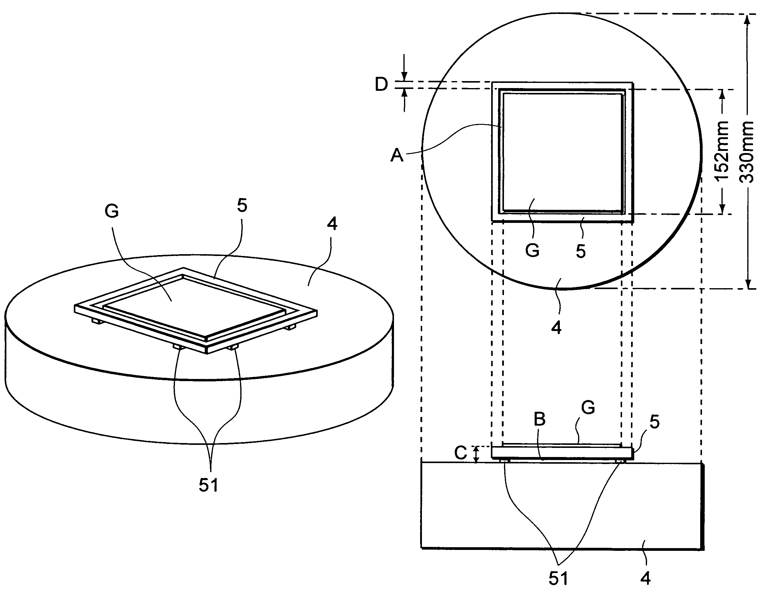
[0081]A square-type substrate having four sides each of which is six inches long and having temperature sensors was placed on a circular heating plate that has a diameter of 330 mm and that is used to heat a semiconductor wafer having a diameter of 12 inches. A frame member made of an aluminum alloy was disposed around the substrate. The substrate was heated at 120° C. by the heating plate and the substrate was kept in a temperature constant state. In that state, the temperatures of the surface of the substrate were detected. At that point, the distance between each of the side surfaces of the substrate and the inner surface of the frame member was 2 mm. The height of the frame member from the front surface of the heating plate was 6 mm. The width of the frame member was 10 mm. The distance between the lower surface of the frame member and the front surface of the heating plate was 0.1 mm. In this example, a heating plate having a diameter of 330 mm was exemplified. However, it shou...

second example

[0087]A square substrate having four sides each of which is six inches long and having temperature sensors was placed on a circular heating plate that has a diameter of 330 mm and that is used to heat a semiconductor wafer having a diameter of 12 inches. A frame member made of an aluminum alloy was disposed around a substrate. The substrate was heated at 150° C. and kept in a temperature constant state by the heating plate. In that state, the temperature on the surface of the substrate were measured. At that point, the substrate was supported by proximity pins disposed on the front surface of the heating plate in such a manner that the substrate floated on the front surface of the heating plate by 80 μm. The distance between each of the side surfaces of the substrate and the inner surface of the frame member was 2 mm. The height of the frame member from the front surface of the heating plate was 6 mm. The width of the frame member was 10 mm. The distance between the lower surface of...

third example

[0090]Except that the substrate was heated at 220° C., an experiment was conducted in the same condition as the second example. FIG. 16A shows a chronological change of measured values of the temperatures of temperature sensors. The range width of the temperatures on the surface of the substrate in a time period from 400 second to 600 seconds after the substrate was heated and the substrate temperature became stable was 1.50° C.


PUM

PropertyMeasurementUnit
diameteraaaaaaaaaa
thicknessaaaaaaaaaa
thicknessaaaaaaaaaa

Abstract

A heat processing apparatus for heating a mask substrate is disclosed. A mask substrate on which a coating solution has been coated is placed on a heating plate that heats the substrate. A frame member is disposed on the heating plate so that the frame member faces a side surface of the mask substrate placed on the heating plate when the frame member is attached to the heating plate and that a clearance is formed between the frame member and the heating plate when the frame member is attached to the heating plate. The frame member suppresses heat radiated from the side surface of the substrate. As a result, the temperature uniformity of the surface of the substrate can be improved. In addition, since the clearance is formed between the frame member and the heating plate, particles do not accumulate in the region. Thus, adhesion of particles to the substrate can be suppressed.

Description

BACKGROUND OF THE INVENTION[0001]1. Field of the Invention[0002]The present invention relates to a heat processing apparatus and a heat processing method for performing a heat process for a substrate such as a mask substrate on which for example a resist solution has been coated.[0003]2. Description of the Related Art[0004]When a semiconductor mask is formed in a fabrication process for a semiconductor device, a resist solution is coated on a square mask substrate. With a photo mask, the resist film is exposed and developed. As a result, a desired resist pattern is formed. As such a substrate, for example a six-inch size square glass substrate having four sides each of which is 152 mm long and having a thickness of 6.35 mm is used.[0005]The resist solution is made by dissolving a component of a coating film in a solvent. After the resist solution is coated on a substrate, a heating process for heating the substrate at a predetermined temperature and evaporating the solvent is prefor...

Claims


Application Information

Patent Timeline
Patent Type & Authority Patents(United States)
IPC IPC(8): B05C11/02B05C11/00B05C13/00B05C13/02F27D3/00H01L21/027G03F7/16H01L21/00H01L21/38
CPCH01L21/67109G03F7/168
Inventor TAKEI, TOSHICHIKAKANEDA, MASATOSHI
Owner TOKYO ELECTRON LTD
Learn More