III-V nitride semiconductor substrate and its production method

Active Publication Date: 2005-03-03
SUMITOMO CHEM CO LTD
View PDF5 Cites 41 Cited by
  • Summary
  • Abstract
  • Description
  • Claims
  • Application Information

AI Technical Summary

Benefits of technology

[0015] Accordingly, an object of the present invention is to provide a self-supported substrate made of a III-V nitride semicond

Problems solved by technology

However, because there are no base substrates having lattice constants matched to those of the nitride semiconductor layers, it is difficult to grow high-quality layers, resulting in nitride semiconductor layers with a lot of crystal defects.
Even by the method of forming the low-temperature-deposited layer, however, the resultant substrates are filled with considerable numbers of crystal defects such as threading dislocations, vacancies, etc., insufficient for obtaining presently demanded high-performance devices.
In an as-grown state, the GaN substrate obtained by the ELO method or the DEEP method usually has morphology such as pits, hillocks, etc. on its surface, resulting in difficulty in growing an epitaxial layer for producing devices without further treatment.
It has been found, however, that the self-supported GaN substrate produced by such a method has a nonuniform carrier concentration on its surface despite the lowered dislocation density.
The nonuniform carrier concentration distribution on its substrate surface is a problem that has never occurred in conventionally used semiconductor substrates of Si and GaAs because of their production methods.
When crystal growth is carried out while forming facets in a growth interface, to lower the dislocation of the self-supported GaN substrate, there inevitably occurs difference between facet planes and other planes, resulting in different rates of crystal growth and thus differences in effective segregation coefficients

Method used


Image

  • III-V nitride semiconductor substrate and its production method
  • III-V nitride semiconductor substrate and its production method
  • III-V nitride semiconductor substrate and its production method

Examples


Example

EXAMPLE 1

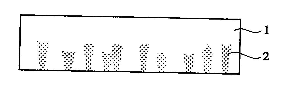
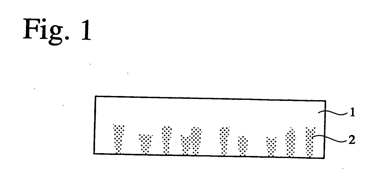
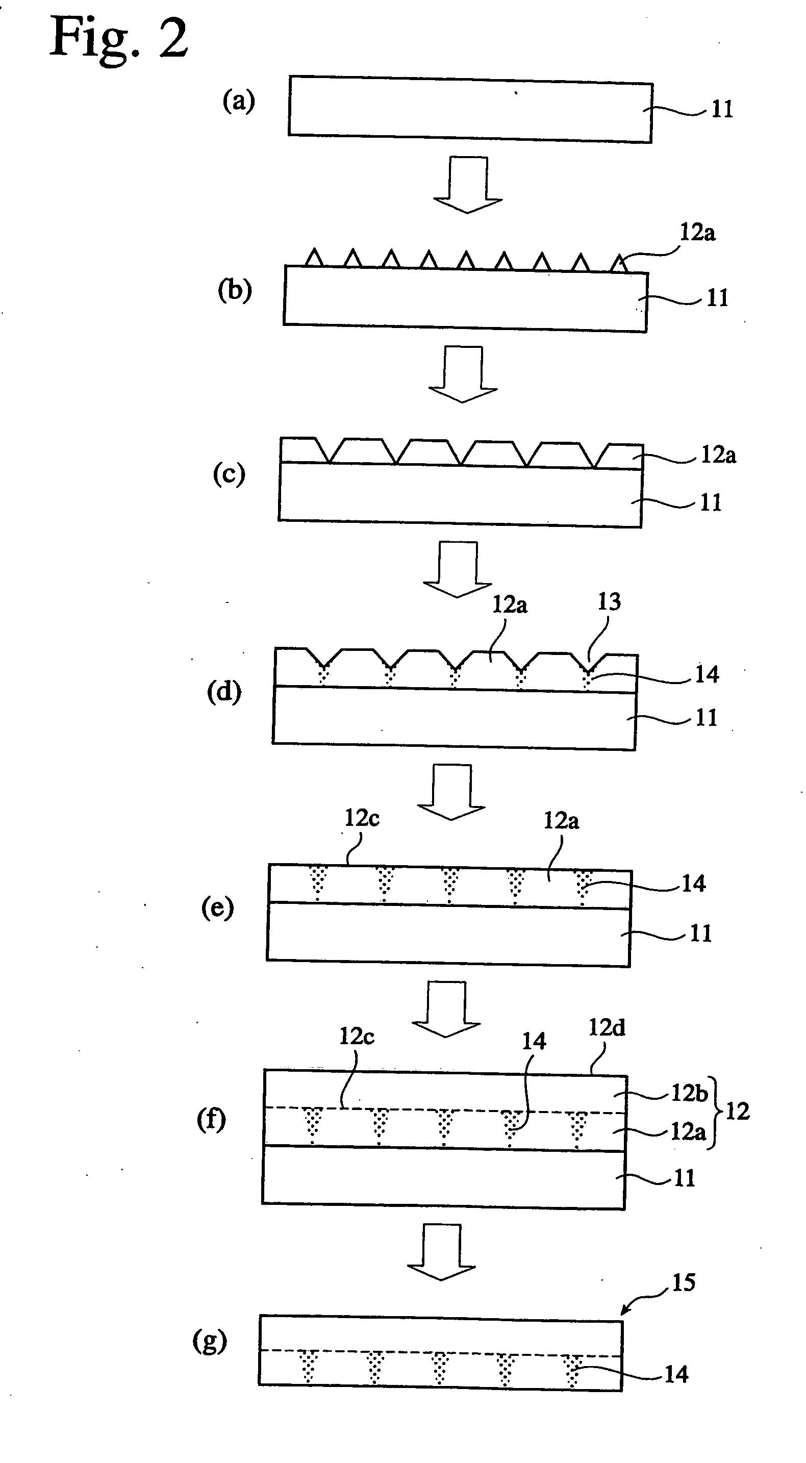
[0077] An epitaxial GaN layer was grown on a sapphire substrate, and the sapphire substrate was then removed to produce and evaluate a self-supported GaN substrate 1 having a layer containing regions 2 having different carrier concentrations and a layer having a substantially uniform carrier concentration as shown in FIG. 1. The production method of the self-supported GaN substrate in this Example will be explained below referring to FIG. 2.

[0078] First, an epitaxial GaN layer 12a was grown on a sapphire substrate 11 by an HVPE method. The HVPE method is a method, in which GaCl, a halide of a group-III element, is transported onto a surface of a heated base substrate, and mixed with NH3 on the base substrate, so that they react with each other to cause the vapor-phase growth of a GaN crystal on the base substrate 11. The source gases are supplied with carrier gases such as H2 and N2. The temperature in a region surrounding the base substrate 11 was set at 1000° C. by an e...

Example

COMPARATIVE EXAMPLE 1

[0088] A thick GaN crystal layer was grown on a sapphire substrate in the same manner as in Example 1 except that the partial pressures of GaCl and NH3 as source gases was 5×10⁻³ atm and 0.3 atm, respectively, on the substrate, and that a carrier gas used was a mixed gas of 2% H2 and 98% N2. As a result, many pits remained unburied on the surface until GaN became as thick as 300 μm.

[0089] This substrate was taken out of the reaction tube, and the sapphire substrate was removed by the above laser lift-off method to obtain a self-supported GaN substrate. Both top and bottom surfaces of the self-supported GaN substrate were mirror-polished to depths of 30 μm and 10 μm, respectively, to improve the flatness of the substrate. By mirror-polishing, almost all pits remaining on the surface of the substrate disappeared. The final thickness of the self-supported GaN substrate was 260 μm.

[0090] The cross section of the self-supported GaN substrate was observed by a fluo...

Example

EXAMPLE 2

[0093] An epitaxial GaN layer was grown on a sapphire substrate substantially in the same manner as in Example 1 except for slight changes in crystal growth conditions in the HVPE method, and the sapphire substrate was removed to produce and evaluate a self-supported GaN substrate shown in FIG. 1. The production method of the self-supported GaN substrate in this Example will be explained below referring to FIG. 2.

[0094] First, an epitaxial GaN layer 12a was grown by the same HVPE method as in Example 1 using a C-plane sapphire substrate 11. The temperature on the substrate was set at 1050° C. by an electric furnace. The partial pressures of GaCl and NH3 as source gases were 6×10⁻³ atm and 0.4 atm, respectively, on the substrate, and the carrier gas used was a mixed gas of 10% H2 and 90% N2 from the initial stage. The GaN crystal was doped with Si by supplying SiH2Cl2 as a doping gas onto the substrate in the process of growing the GaN crystal.

[0095] First, nuclei of the ...


PUM


Abstract

A self-supported III-V nitride semiconductor substrate having a substantially uniform carrier concentration distribution in a surface layer existing from a top surface to a depth of at least 10 μm is produced by growing a III-V nitride semiconductor crystal while forming a plurality of projections on a crystal growth interface at the initial or intermediate stage of crystal growth; conducting the crystal growth until recesses between the projections are buried, so that the crystal growth interface becomes flat; and continuing the crystal growth to a thickness of 10 μm or more while keeping the crystal growth interface flat.

Description

FIELD OF THE INVENTION [0001] The present invention relates to a III-V nitride semiconductor substrate having a low dislocation density and a substantially uniform surface carrier concentration distribution, and a method for producing it. BACKGROUND OF THE INVENTION [0002] Because nitride semiconductor materials have sufficiently wide forbidden bands with direct interband transition, their applications to short-wavelength light-emitting devices have been widely investigated. In addition, because of a large saturated drift velocity of electrons and the usability of a two-dimensional carrier gas in heterojunctions, their applications to electron devices are expected. [0003] Nitride semiconductor layers for constituting these devices are obtained by epitaxial growth on base substrates by vapor phase growth methods such as a metal-organic vapor-phase epitaxy method (MOVPE), a molecular beam epitaxy method (MBE), a hydride vapor-phase epitaxy method (HVPE), etc. However, because there ar...

Claims


Application Information

Patent Timeline
IPC IPC(8): C30B25/18C30B29/40H01L21/20H01L21/205
CPCC30B25/18C30B29/403H01L21/0242H01L21/02458H01L21/02491H01L21/02647H01L21/02513H01L21/0254H01L21/0262H01L21/02639H01L21/02502
Inventor SHIBATA, MASATOMO
Owner SUMITOMO CHEM CO LTD
Why Eureka
Try Eureka