Epitaxy base plate in use for solid-state semiconductor device, solid-state semiconductor device, and preparation method

A technology of epitaxial substrates and semiconductors, which is applied in semiconductor/solid-state device manufacturing, semiconductor devices, semiconductor lasers, etc., can solve the problems of increasing equipment costs and time costs, and achieve the effects of reducing dislocation density, reducing time costs, and simplifying the production process.

Inactive Publication Date: 2006-07-05
龚志荣
View PDF0 Cites 6 Cited by
  • Summary
  • Abstract
  • Description
  • Claims
  • Application Information

AI Technical Summary

Problems solved by technology

[0010] Although the previously mentioned patent documents and papers mentioned above can reduce the penetrating dislocation formed in the epitaxial film during the epitaxy process, whether it is to form a patterned substrate or to form a patterned non-dislocation on the epitaxial film Crystal film requires the use of lithography equipment and process, therefore, it also increases equipment cost and time cost virtually

Method used


Image

  • Epitaxy base plate in use for solid-state semiconductor device, solid-state semiconductor device, and preparation method
  • Epitaxy base plate in use for solid-state semiconductor device, solid-state semiconductor device, and preparation method
  • Epitaxy base plate in use for solid-state semiconductor device, solid-state semiconductor device, and preparation method

Examples


Embodiment Construction

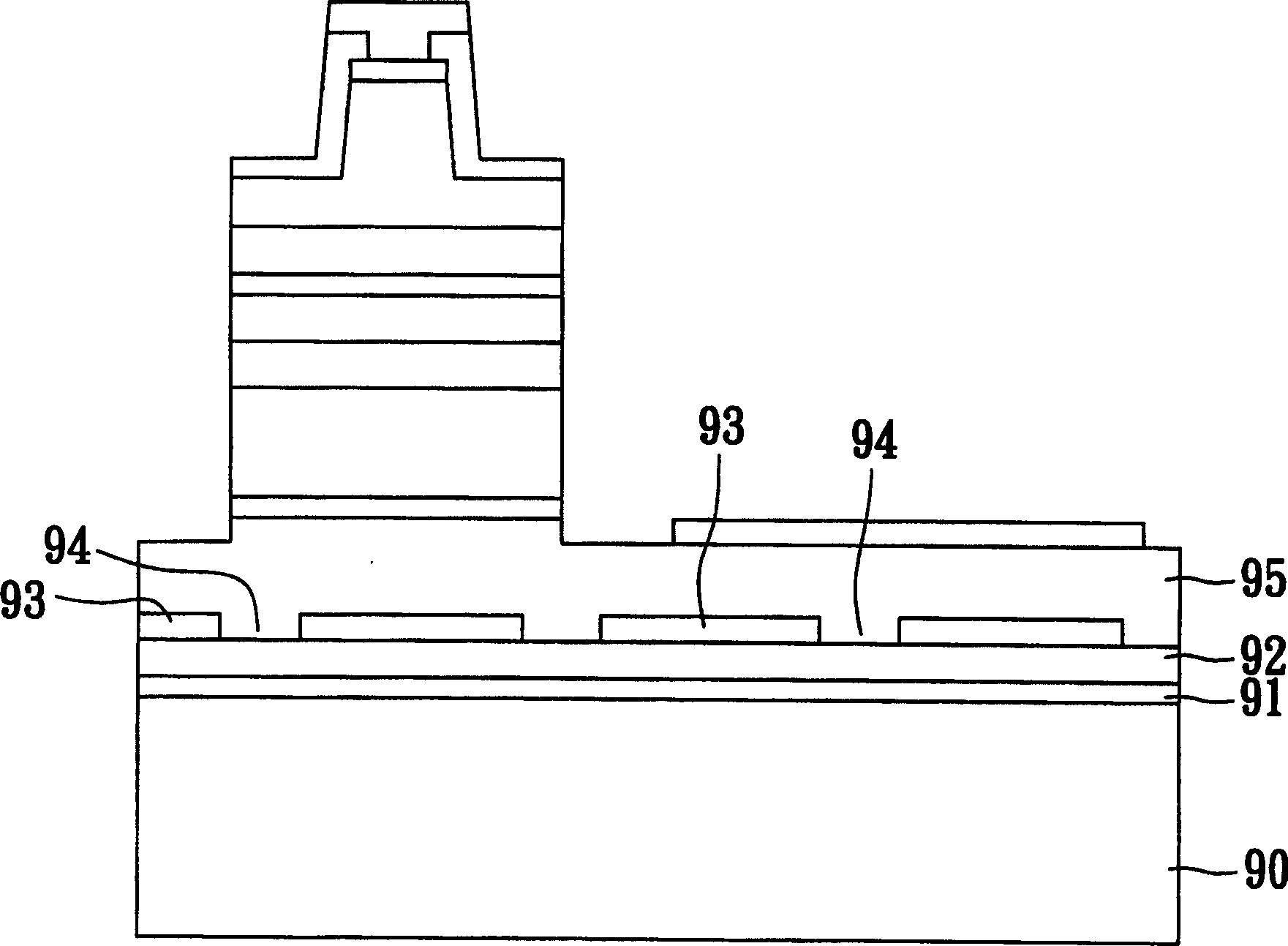
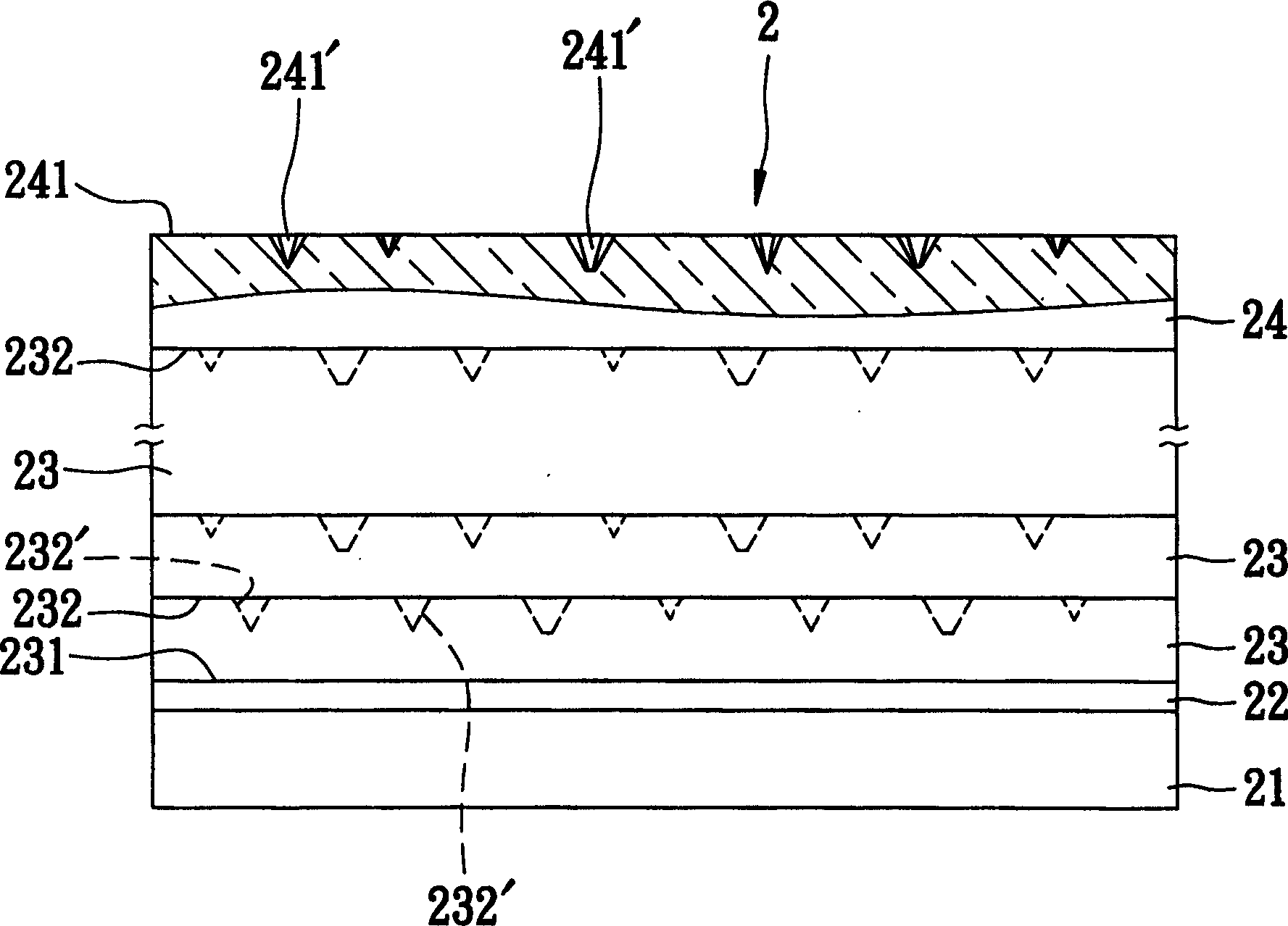
[0081] refer to image 3 and Figure 5 , In a specific embodiment of the present invention, the solid-state semiconductor device includes: an epitaxial substrate 2 and an emitting unit 3 formed on the epitaxial substrate 2 .

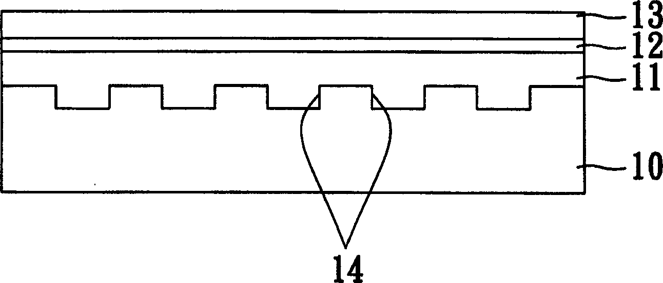
[0082] The epitaxial substrate 2 has a board body 21, a buffer film 22 connected to the board body 21, a second second groove 241' formed on the buffer layer 22 and having a plurality of hexagonal grooves 241' with irregular sizes. The epitaxial film 24 , and a plurality of first epitaxial films 23 sandwiched between the second epitaxial film 24 and the buffer film 22 and having a plurality of hexagonal grooves 232 ′ with irregular sizes. In this embodiment, the board body 21 is made of sapphire with a hexagonal crystal structure, and the epitaxial films 23 and 24 are made of gallium nitride (GaN).

[0083] In the emitting unit 3 of this embodiment, the first type semiconductor layer 311 is made of n-GaN, and the light emitting layer 312 is a multilayer ...


PUM


Abstract

Epitaxy base plate in use for solid-state semiconductor device includes a plate itself, a buffer film connected to the plate itself, at least a first surface connected to the buffer film, and first epitaxial film of coarse second surface in irregular change opposite to the first surface. The solid-state semiconductor device includes the said epitaxy base plate, and an emission unit setup at side of epitaxy base plate. Te invention also discloses a preparing method. Features of the invention are: simplifying preparing procedure, reducing cost of time, and reducing dislocation density largely by increasing number of epitaxial film with coarse surface in order to improve optical character of the prepared epitaxial film and the solid-state semiconductor device.

Description

technical field [0001] The present invention relates to a semiconductor device and a manufacturing method thereof, in particular to an epitaxy substrate for a solid-state semiconductor device, a solid-state semiconductor device and a manufacturing method thereof. Background technique [0002] Currently common solid-state semiconductor devices generally include light-emitting diode (LED) devices, laser diode (LD) devices, or semiconductor radio frequency (radio frequency) devices. Generally speaking, the aforementioned LED devices, LD devices, and semiconductor radio frequency devices are composed of an epitaxial substrate and a semiconductor element formed on the epitaxial substrate (for example: a radio frequency element, or a light emitting element containing a p-n junction (junction)) constituted. [0003] For example, the basic blue or green LED structure is composed of a sapphire substrate, a buffer layer formed on the sapphire substrate, an n-type gallium nitride form...

Claims


Application Information

Patent Timeline
Patent Type & Authority Applications(China)
IPC IPC(8): H01L21/02H01L21/84H01L27/12H01L33/00H01S5/00
Inventor 龚志荣蔡雨利林泰源
Owner 龚志荣
Why Eureka
Try Eureka