Method for manufacturing group III nitride single crystals

Active Publication Date: 2010-05-06
NGK INSULATORS LTD
View PDF3 Cites 10 Cited by
  • Summary
  • Abstract
  • Description
  • Claims
  • Application Information

AI Technical Summary

Benefits of technology

[0014]The present inventors have formed the underlying film composed of the group III nitride on the substrate by vapor phase deposition, removed the underlying film therefrom and roughened the surface of the substrate by heating the substrate and the underlying film in the presence of hydrogen (in-situ etching). Subsequently, the inventors have formed the seed crystal film composed of the group III nitride single crystal on the surface of the substrate by vapor phase deposition. Thereafter, the inventors have proved that, when the group III nitride single crystal is grown on the seed crystal film by the flux method, single crystals having excellent crystallinity and a low dislocation density can be obtained with high productivity.
[0015]Furt

Problems solved by technology

According to the method described in Japanese Patent Laid-open Publication No. 2000-327495A, for example, it is difficult to separate t

Method used


Image

  • Method for manufacturing group III nitride single crystals
  • Method for manufacturing group III nitride single crystals
  • Method for manufacturing group III nitride single crystals

Examples


Example

Example 1

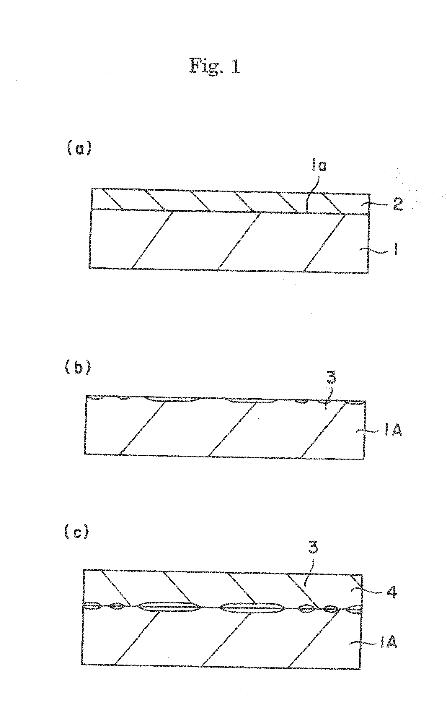
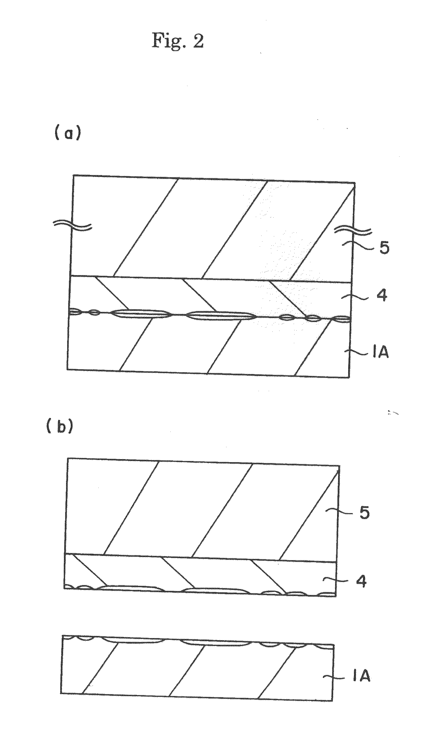
[0039]A c-plane GaN single crystal self-standing substrate was manufactured using the method described with reference to FIGS. 1 and 2.

(Manufacture of Underlying Film)

[0040]A c-plane sapphire substrate 1 with a diameter of 2 inches was put in an MOCVD furnace (metal organic chemical vapor deposition furnace), and heated at 1150° C. for 10 minutes in hydrogen atmosphere to perform the cleaning of the substrate surface. Then, the substrate temperature was reduced to 500° C., and the GaN film was grown to a thickness of 0.03 μm using TMG (trimethyl gallium) and ammonia as raw materials. Next, the substrate temperature was raised up to 1100° C., and the GaN single crystal underlying film 2 was grown to a thickness of 0.5 pm using TMG (trimethyl gallium) and ammonia as raw materials.

(In-situ Etching)

[0041]This substrate was heated again at 1150° C. for 15 minutes in hydrogen atmosphere, and the surface GaN film 2 was almost evaporated to expose the sapphire substrate 1A. It was ...

Example

Example 2

[0046]An a-plane GaN single crystal self-standing substrate was manufactured using the method described with reference to FIGS. 1 and 2.

(Manufacture of Underlying Film)

[0047]An r-plane sapphire substrate 1 with a diameter of 2 inches was put in an MOCVD furnace (metal organic chemical vapor deposition furnace), and heated at 1150° C. for 10 minutes in hydrogen atmosphere to perform the cleaning of the substrate surface. Next, the substrate temperature was reduced to 500° C., and a GaN film was grown to a thickness of 0.03 μm using TMG (trimethyl gallium) and ammonia as raw materials. Next, the substrate temperature was raised up to 1100° C., and the GaN single crystal underlying film 2 was grown to a thickness of 0.5 pm using TMG (trimethyl gallium) and ammonia as raw materials.

(In-Situ Etching)

[0048]This substrate was heated again at 1150° C. for 30 minutes in hydrogen atmosphere, and the surface GaN film 2 was almost evaporated to expose the sapphire substrate 1A. It was ...

Example

Example 3

[0052]An m-plane GaN single crystal self-standing substrate was manufactured using the method according to the present invention described with reference to FIGS. 1 and 2.

(Manufacture of Underlying Film)

[0053]An m-plane sapphire substrate 1 with a diameter of 2 inches was put in an MOCVD furnace (metal organic chemical vapor deposition furnace), and heated at 1150° C. for 10 minutes in hydrogen atmosphere to perform the cleaning of a substrate surface. Next, the substrate temperature was reduced to 500° C., and the GaN film was grown to a thickness of 0.03 μm using TMG (trimethyl gallium) and ammonia as raw materials. Next, the substrate temperature was raised up to 1100° C., and the GaN single crystal underlying film 2 was grown to a thickness of 0.5 pm using TMG (trimethyl gallium) and ammonia as raw materials.

(In-Situ Etching)

[0054]This substrate was heated again at 1150° C. for 30 minutes in hydrogen atmosphere, and the surface GaN film 2 was almost evaporated to expose...


PUM


Abstract

An underlying film 2 of a group III nitride is formed on a substrate 1 by vapor phase deposition. The substrate 1 and the underlying film 2 are subjected to heat treatment in the present of hydrogen to remove the underlying film 2 so that the surface of the substrate 1 is roughened. A seed crystal film 4 of a group III nitride single crystal is formed on a surface of a substrate 1A by vapor phase deposition. A group III nitride single crystal 5 is grown on the seed crystal film 4 by flux method.

Description

TECHNICAL FIELD OF THE INVENTION[0001]The present invention relates to a method for growing a group III nitride single crystal.BACKGROUND ART[0002]Gallium nitride (GaN)-based thin film crystal draws attention as excellent blue light-emitting devices, has been used as a material for light-emitting diodes and expected as a blue-violet semiconductor laser device for an optical pickup. In recent years, the GaN thin film crystal draws attention as a semiconductor film composing an electronic device, such as a high-speed IC chip for use in cellular phones.[0003]There is reported a method for depositing a seed crystal film of GaN or AlN on a single crystal substrate composed of sapphire to obtain a template substrate, and growing a GaN single crystal on the template substrate (see Japanese Patent Laid-open Publication No. 2000-327495A).[0004]According to Formation chemistry of high-density nanocraters on the surface of sapphire substrates with an in-situ etching and growth mechanism of dev...

Claims


Application Information

Patent Timeline
IPC IPC(8): C30B7/00
CPCC30B23/02C30B25/02C30B25/20C30B29/403C30B29/406
Inventor KURAOKA, YOSHITAKASUMIYA, SHIGEAKIMIYOSHI, MAKOTOIMAEDA, MINORU
Owner NGK INSULATORS LTD
Why Eureka
Try Eureka