Method of manufacturing a semiconductor device

Inactive Publication Date: 2008-02-12
SEMICON ENERGY LAB CO LTD
View PDF47 Cites 3 Cited by
  • Summary
  • Abstract
  • Description
  • Claims
  • Application Information

AI Technical Summary

Benefits of technology

[0014]The present invention has been made in view of the above, and an object of the present invention is to provide an insulated gate field effect trans

Problems solved by technology

However, when the TFT does not receive channel doping, the off leak current tends to increase as the thickness of the semiconductor layer is increased, resulting in insufficient ON/OFF ratio.
However, this measure becomes difficult as the thickness of the semiconductor layer is increased.
In particular, in a region located deep in the semiconductor layer, acceptor ions have to be implanted at high acceleration voltage, causing damage in crystals and lowering of the crystallinity.
Furthermore, if the acceptor

Method used


Image

  • Method of manufacturing a semiconductor device
  • Method of manufacturing a semiconductor device
  • Method of manufacturing a semiconductor device

Examples


Example

EMBODIMENT 1

[0048]FIGS. 7A to 7E are diagrams illustrating a method of manufacturing a semiconductor device according to Embodiment 1 of the present invention. As shown in FIG. 7A, a base insulating film 102 is formed on a substrate 101 from a single layer or a laminate of a silicon nitride film, a silicon oxide film, and a silicon nitroxide film. The material of the substrate 101 is a commercially-available glass material called non-alkaline glass such as alminosilicate glass. Alternatively, a semiconductor substrate such as a single crystal silicon substrate may be employed.

[0049]An amorphous semiconductor layer 103 is formed from an amorphous material such as silicon or silicon doped with germanium. The thickness of the amorphous semiconductor layer 103 is 60 to 200 nm, typically 150 nm. A metal-containing layer 104 contains a metal element having a catalytic action that makes it possible to crystallize the amorphous semiconductor layer at a temperature not higher than 600° C. an...

Example

EMBODIMENT 2

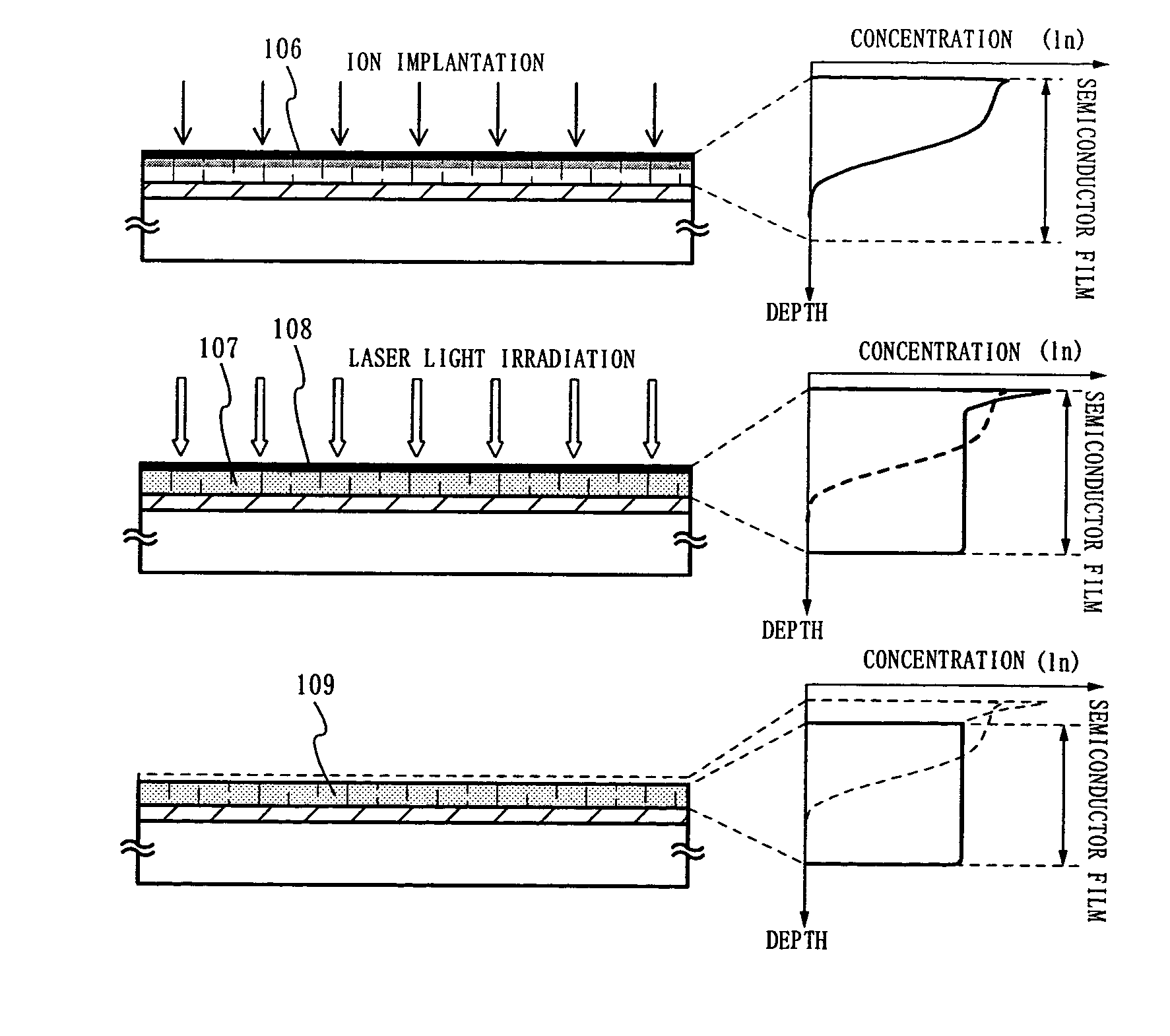
[0057]FIGS. 8A to 8D are diagrams illustrating a method of manufacturing a semiconductor device according to Embodiment 2 of the present invention. As shown in FIG. 8A, a base insulating film 102 and an amorphous semiconductor layer 103 are formed on a substrate 101.

[0058]First, ions are implanted in the amorphous semiconductor layer 103 for channel doping. When ions of an impurity of one conductivity type are accelerated by electric filed and implanted into a semiconductor layer, the impurity element implanted is distributed in accordance with the acceleration voltage. With such ions implanted at 30 kV or less, the concentration in an impurity implanted region 110 peaks in the vicinity of the surface and decreases as the distance from the surface is increased to form a distribution resembling Gaussian distribution as shown in an inserted diagram of FIG. 8B. The concentration of the implanted impurity in the semiconductor layer is 1×10¹⁵ to 5×10¹⁸ / cm3 at its peak.

[0059]T...

Example

EMBODIMENT 3

[0063]FIGS. 9A to 9E are diagrams illustrating a method of manufacturing a semiconductor device according to Embodiment 3 of the present invention. As shown in FIG. 9A, a base insulating film 102 and an amorphous semiconductor layer 103 are formed on a substrate 101.

[0064]First, the amorphous semiconductor layer 103 is irradiated with pulse laser light to be crystallized. The light source of the pulse laser light can be a pulse oscillation gas laser or solid-state laser Specifically, an excimer laser oscillator, a YAG laser oscillator, a YVO4 laser oscillator, a YLF laser oscillator, or the like is employable. The oscillation frequency is set to 10 to 300 Hz and the oscillation pulse width is set to 20 to 100 nsec. A region of the amorphous semiconductor layer that is irradiated with the pulse laser light is partially or entirely melted and crystallized. The resultant crystalline semiconductor film, which is denoted by 114, has an irregular surface and the largest level ...


PUM


Abstract

An impurity of one conductivity type is ionized and accelerated by electric field before being implanted into a semiconductor layer to form a high concentration impurity region near its surface. Then the semiconductor layer is irradiated with continuous wave laser light for melting and crystallization or recrystallization, through which a region where the concentration of the impurity is constant is formed in the semiconductor layer. The continuous wave laser light irradiation may bring the semiconductor layer to the crystalline phase from the amorphous phase as long as the impurity element is re-distributed. The impurity is segregated through this process to newly create a high concentration region. However, this region is removed and no problem arises.

Description

BACKGROUND OF THE INVENTION[0001]1. Field of the Invention[0002]The present invention relates to a semiconductor device with a crystalline semiconductor layer formed on an insulating surface, and particularly to a semiconductor device in which an insulating gate field effect transistor is constructed with a crystalline semiconductor layer being crystallized by laser light irradiation.[0003]2. Description of the Related Art[0004]Technologies of manufacturing an insulating gate field effect transistor by forming an amorphous silicon film on a substrate with an insulating surface and crystallizing the film by laser light irradiation are applied to active matrix liquid crystal display devices, typically flat surface type display devices (flat panel displays).[0005]An example of crystallizing an amorphous semiconductor layer by laser light irradiation is polycrystallization technology, in which a thin film transistor (TFT) is manufactured by irradiating the second harmonic of laser light...

Claims


Application Information

Patent Timeline
IPC IPC(8): H01L21/425G02F1/1368H01L21/20H01L21/268H01L21/336H01L21/77H01L21/84H01L27/12H01L29/49H01L29/786
CPCH01L21/2026H01L21/268H01L27/12H01L27/1285H01L29/66757H01L29/78675H01L29/4908H01L21/02686H01L21/02422H01L21/02488H01L21/02532H01L21/02505H01L21/02672H01L21/02381H01L21/02683
Inventor SHIMOMURA, AKIHISANAKAMURA, OSAMUARAO, TATSUYAMIYAIRI, HIDEKAZUISOBE, ATSUOTAKANO, TAMAEINOUE, KOUKI
Owner SEMICON ENERGY LAB CO LTD
Why Eureka
Try Eureka