Semiconductor device and method for manufacturing the same

Inactive Publication Date: 2007-12-20
KK TOSHIBA
View PDF0 Cites 5 Cited by
  • Summary
  • Abstract
  • Description
  • Claims
  • Application Information

AI Technical Summary

Benefits of technology

[0014]The present invention has been made in view of these circumstances, and an object thereof is to provide a semiconductor

Problems solved by technology

However, the crystallinity of the epitaxially grown layer formed in this manner is poorer than the crystallinity of a SOI substrate formed by a bonding method, and the epitaxially grown layer is not suited for practical use.
However, the reduction in device size is about to reach the limit.
As a result, the production processing temperatures of the respective devices are different, causing a processing temperature mismatch, which poses difficulties in the device production.
As a result, the crystallinity of Ge in the vicinity of the interface between the Si substrate and the Ge region is poor, and a device should be formed in a region other than this region.
Because of this, the area in which a device can be formed is reduced, and high integration of devices cannot be expected.
20.7 (2005) is concerned, the improvement of crystallinity is limited, and the poor crystallinity remains a problem in terms of yield.
As epitaxial growth reflects the cr

Method used


Image

  • Semiconductor device and method for manufacturing the same
  • Semiconductor device and method for manufacturing the same
  • Semiconductor device and method for manufacturing the same

Examples


Example

First Embodiment

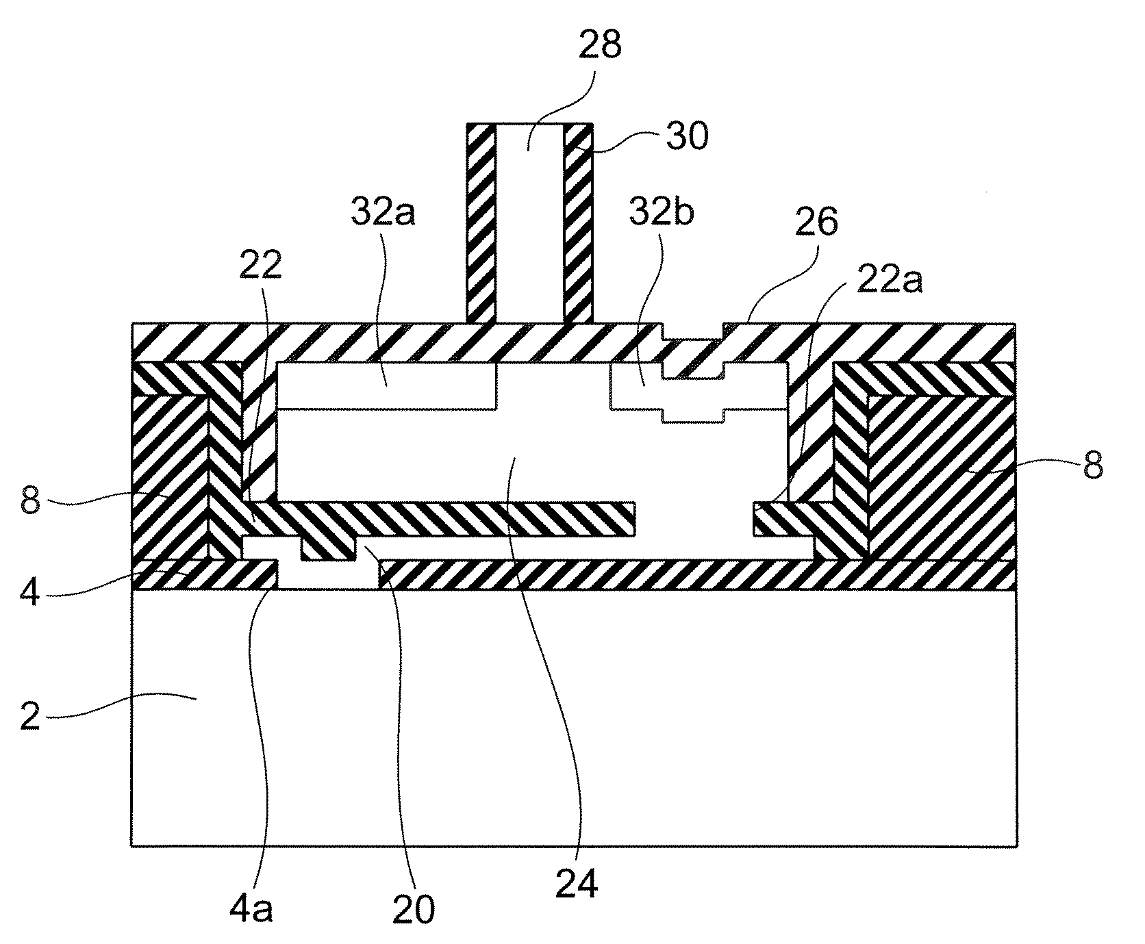
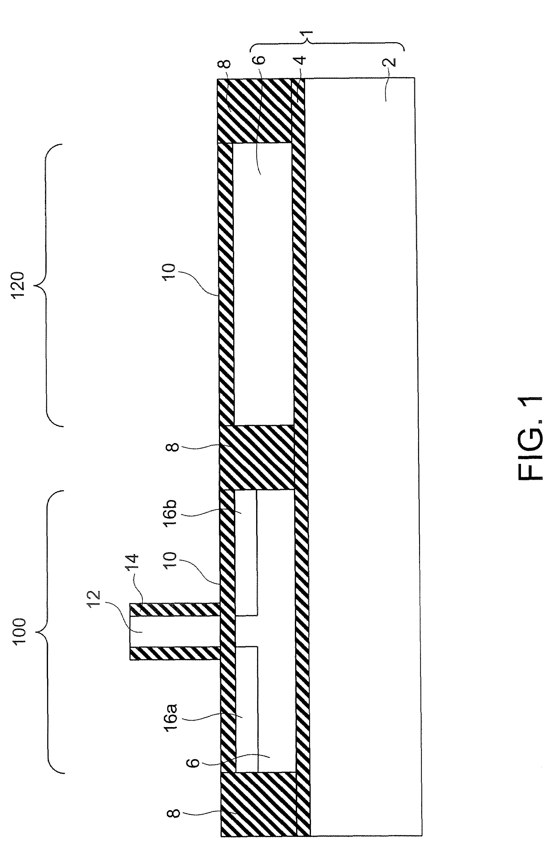
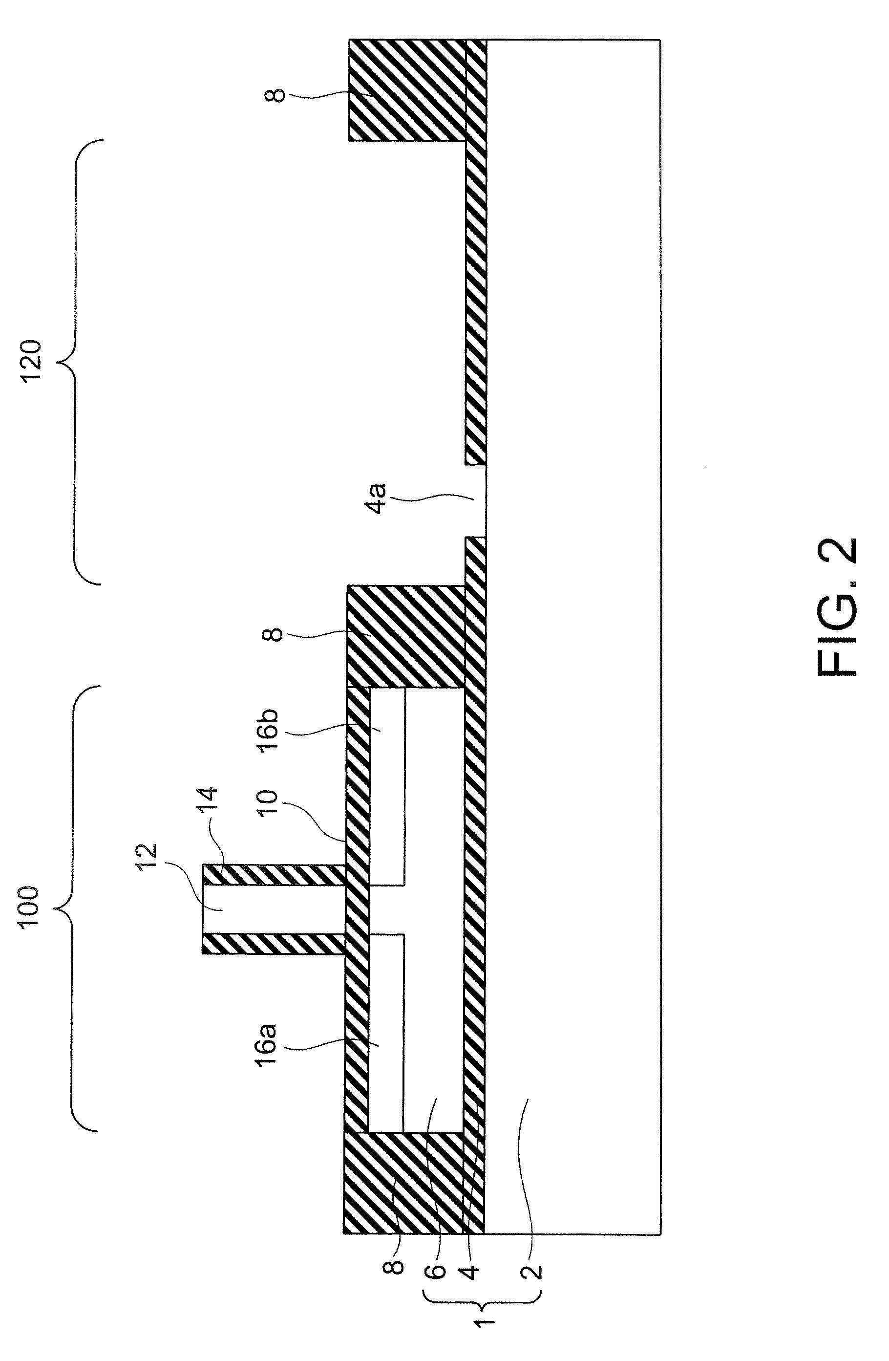
[0029]Referring to FIGS. 1 through 8, a semiconductor device in accordance with a first embodiment of the present invention is described. The semiconductor device of this embodiment has a structure in which a SOI substrate is formed with a supporting substrate and a SOI layer having different plane orientations from each other, an n-type MOSFET is formed on the SOI layer, a Ge layer is formed by virtue of the plane orientation of the supporting substrate, and a p-type MOSFET is formed on the Ge layer. In the following, a method for manufacturing the semiconductor device of this embodiment is described.

[0030]First, as shown in FIG. 1, a SOI substrate 1 that includes a supporting substrate 2 made of single-crystal silicon having the (110) plane orientation, a buried oxide film (BOX layer) 4, and a SOI layer 6 made of single-crystal silicon having the (100) plane orientation, is prepared. After STI (Shallow Trench Isolation) layers 8 for isolating each region 100 in whi...

Example

Second Embodiment

[0044]Referring now to FIG. 9, a semiconductor device in accordance with a second embodiment of the present invention is described.

[0045]The semiconductor device of this embodiment is substantially the same as the semiconductor device of the first embodiment, except that the film thickness M of the epitaxially grown layer 20 and the distance L in the film plane direction between the opening 22a formed in the insulating film 22 and the opening 4a formed in the buried oxide film layer 4 satisfies the following conditions. More specifically, there is relationship between the film thickness tep of the epitaxially grown layer 20 and the distance L between openings formed in the insulating films 4 and 22:

tep×tan θ

[0046]where θ represents the angle of a (111) plane to be a slip plane 40 with respect to the film plane of the epitaxially grown layer 20. In a case where the epitaxially grown layer 20 has a (100) plane orientation, the angle θ is 54.7°. In a case where it has ...

Example

Third Embodiment

[0048]Referring now to FIG. 10, a semiconductor device in accordance with a third embodiment of the present invention is described.

[0049]The semiconductor device of this embodiment is substantially the same as the semiconductor device of the first embodiment, except that there is the following relationship among the film thickness tep of the epitaxially grown layer 20, the thickness tin of the insulating film 4, and the opening width w1 of the opening 4a formed in the buried oxide film layer 4:

(tin+tep)≧w1×tan θ

[0050]With this arrangement, at least a part of the opening 22a formed in the insulating film 22 exists vertically above the opening 4a.

[0051]Here, θ represents the angle of the (111) plane 40 with respect to the epitaxially grown layer 20. In a case where the epitaxially grown layer 20 has the (100) plane orientation, the angle θ is 54.7°. In a case where it has the (110) plane orientation, the angle θ is 35.3°. In a case where it has the (111) plane orienta...


PUM


Abstract

It is made possible to obtain epitaxially grown layers with excellent crystallinity. A semiconductor device includes: a semiconductor layer having crystallinity; a first insulating film formed on the semiconductor layer and having a first opening to reach the semiconductor layer; a first epitaxially grown layer formed on the first insulating film so as to embed the first opening; a second insulating film formed on the first epitaxially grown layer and having a second opening to reach the first epitaxially grown layer; and a second epitaxially grown layer formed on the second insulating film so as to embed the second opening.

Description

CROSS-REFERENCE TO RELATED APPLICATION[0001]This application is based upon and claims the benefit of priority from prior Japanese Patent Application No. 2006-168738 filed on Jun. 19, 2006 in Japan, the entire contents of which are incorporated herein by reference.BACKGROUND OF THE INVENTION[0002]1. Field of the Invention[0003]The present invention relates to a semiconductor device and a method for manufacturing the semiconductor device.[0004]2. Related Art[0005]There have been known techniques for forming semiconductor crystal layers on insulating films such as SiO2 films. Devices formed on SiO2 films are known as SOI (silicon on insulator) devices, and have been used as low-power-consumption devices in recent years. SOI substrates to be used in SOI devices are produced by methods involving the entire substrate surface, such as a bonding method, the SIMOX method, and the ELTRAN method. Such SOI substrates have been put on the market. A single-crystal region of Si on a SiO2 film in a...

Claims


Application Information

Patent Timeline
IPC IPC(8): H01L27/12H01L21/20H01L21/84
CPCH01L21/84H01L27/12H01L29/78684H01L29/78681H01L29/045
Inventor KAMATA, YOSHIKI
Owner KK TOSHIBA
Why Eureka
Try Eureka