Optical system and apparatus and method for making semiconductor device using same

An optical system and semiconductor technology, applied in chemical instruments and methods, semiconductor devices, semiconductor/solid-state device manufacturing, etc., can solve problems such as cross-sections that are not suitable for the width direction

Inactive Publication Date: 2004-04-14
MITSUBISHI ELECTRIC CORP
View PDF2 Cites 0 Cited by
  • Summary
  • Abstract
  • Description
  • Claims
  • Application Information

AI Technical Summary

Problems solved by technology

However, the existing optical system for forming a linear beam is not suitable for selecting a cross section in the width direction.
In addition, it is impossible to condense the width direction of the linear beam to the extreme fineness by performing homogenization in two orthogonal directions at the same time.

Method used


Image

  • Optical system and apparatus and method for making semiconductor device using same
  • Optical system and apparatus and method for making semiconductor device using same
  • Optical system and apparatus and method for making semiconductor device using same

Examples


Embodiment 1

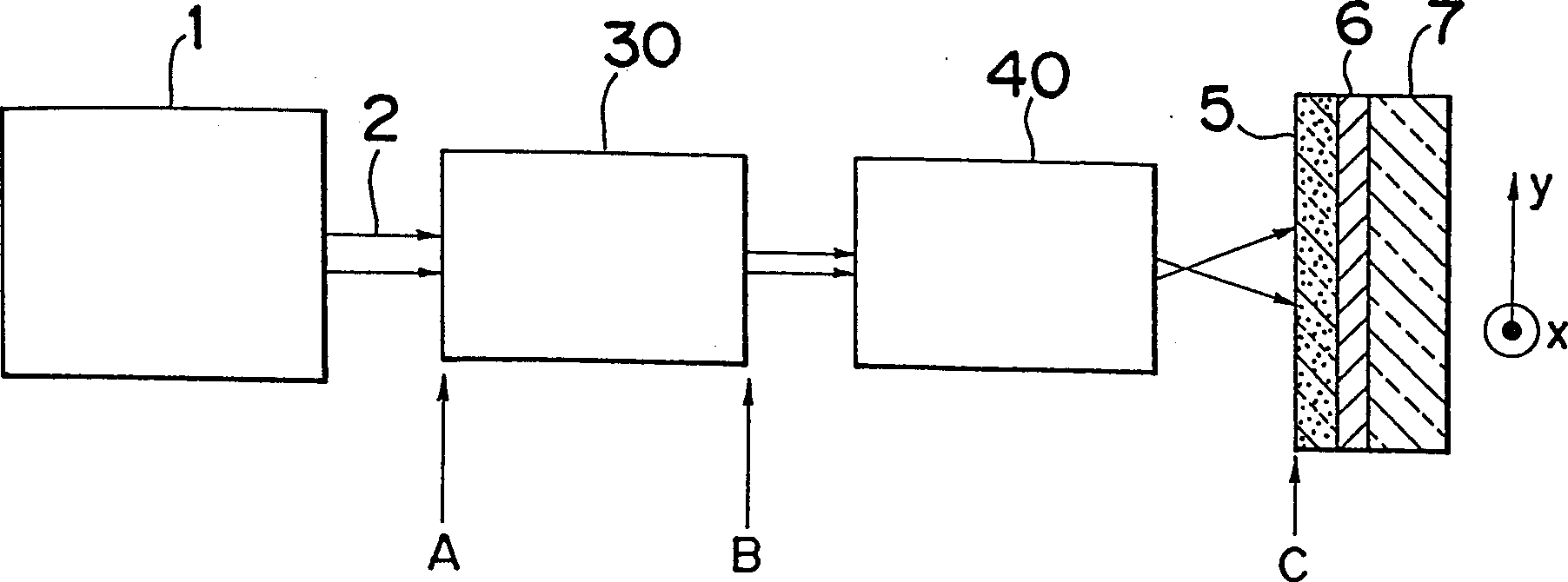
[0058] Figure 3A and 3B Showing the structure of the optical system for laser heat treatment according to the embodiment of the present invention, the intensity distribution shaping device 30 uses a light-transmitting device having a small tapered total reflection surface at the front. In the intensity distribution shaping device 30, a wedge-shaped device 31 formed of a light-transmitting material or a pair of obliquely opposite mirror pairs can be used.

[0059] Hereinafter, an example of a wedge-shaped device 31 is shown, and the wedge-shaped device 31 is a tapered part (block) forming a wedge, such as Figure 3A As shown, only on the front side, reduce the thickness in the y direction, and in the x direction, as Figure 3B As shown, the thickness is constant.

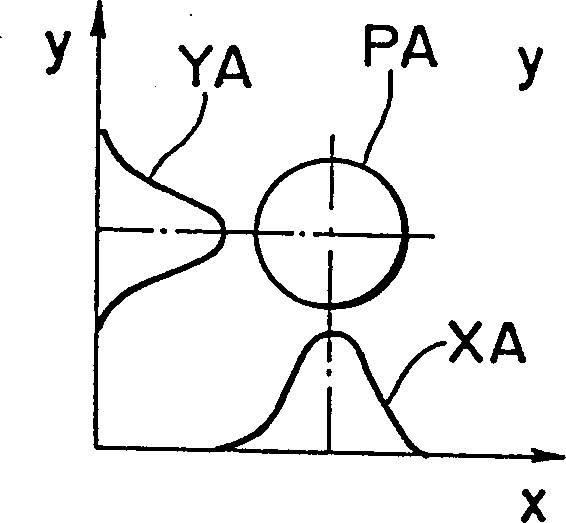
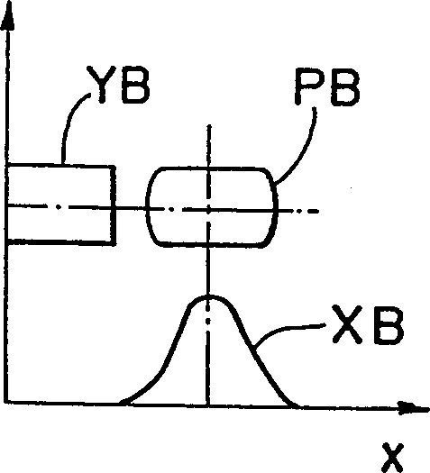
[0060] The oscillating laser light 2 incident from the laser oscillator 1 to the incident surface on the wide side of the component is reflected by the y-direction tapered surface of the component. Therefore, os...

Embodiment 2

[0064] In this embodiment, the intensity distribution shaping means utilizes a lens 32 for light collection and a waveguide 33 with a pair of reflective surfaces facing the front side of the lens 32 .

[0065] As for the waveguide 33, a light-transmitting member that is totally reflected on both surfaces, or a mirror body in which a pair of mirror surfaces face each other can be used.

[0066] The lens 32 is a condensing lens for injecting laser light from the oscillator into the waveguide 33, and as this lens, a spherical lens or a (cylindrical) lens that converges or diverges in the y direction is used.

[0067] Hereinafter, in an example of the intensity distribution shaping device 30, as Figure 4A and 4B As shown in FIG. 2 , a combination of a spherical lens as the lens 32 and a translucent narrow-width member as the waveguide 33 is shown. In this example, the component uses a pair of wide surfaces perpendicular to the width direction (y direction) as the reflection sur...

Embodiment 3

[0071] In another embodiment, the intensity distribution shaping device 30 of the optical system for laser heat treatment is made up of a segmented (cylindrical) cylindrical lens 34, which is as Figure 5A As shown in and 5B, a (cylindrical) cylindrical lens is divided into two parts, that is, two half (cylindrical) cylindrical lenses separated from each other.

[0072] Such as Figure 5A As shown, a pair of split (cylindrical) cylindrical lenses 34 split in the y direction has its longitudinal direction facing the x direction, and the oscillating laser light 2 emitted from the laser oscillator 1 is split into and refracted by these semi-cylindrical lenses. The peripheral part of the beam and the central part of the beam directly entering the gap between the two semi-cylindrical lenses. The split beam superimposes the peripheral light and the central light on the entrance surface of the beam shaper 40 to form a substantially uniform intensity distribution. On the other hand,...


PUM

PropertyMeasurementUnit
thicknessaaaaaaaaaa

Abstract

An optical system that controls laser beam spot profile for forming a high performance thin film by a laser heat treatment process is provided. In the optical system that irradiates a rectangular laser beam on a film formed on a substrate, intensity distribution forming means makes the intensity distribution uniform in the longitudinal direction while maintaining the properties of the laser beam such as directivity in the direction of shorter side, thereby making it possible to concentrate the light to a limit permitted by the nature of the laser beam and achieve the maximum intensity gradient on the film disposed on the substrate. Thus a steep temperature distribution can be generated on the film disposed on the substrate and, as a result, high performance thin film can be formed.

Description

technical field [0001] In particular, the present invention relates to an optical system and device for laser heat treatment of a silicon thin film formed on a heat-treated substrate for heat-treating an amorphous or polycrystalline silicon film to polysiliconize it, and a method of manufacturing a semiconductor device using the optical system . Background technique [0002] The pixel part of the liquid crystal panel is composed of switching thin film transistors made of amorphous or polycrystalline silicon films on glass or synthetic quartz substrates. If the driving circuit for driving the pixel transistors (mainly installed outside) can be formed on the panel at the same time, there will be outstanding advantages in terms of manufacturing cost and reliability of the liquid crystal panel. [0003] However, at present, since the silicon film constituting the active layer of the transistor has poor crystallinity, thin film transistors have poor performance as represented by...

Claims


Application Information

Patent Timeline
Patent Type & Authority Patents(China)
IPC IPC(8): H01L21/324H01L21/20B23K26/06B23K26/073H01L21/268
CPCH01L21/2026B23K26/0732B23K2201/40B23K2101/40H01L21/02686H01L21/0242H01L21/02691H01L21/02488H01L21/02422H01L21/02678H01L21/02532H01L21/324H01L21/02675
Inventor 岡本達樹小川哲也古田啓介时岡秀忠笹川智宏西前顺一井上満夫佐藤行雄
Owner MITSUBISHI ELECTRIC CORP
Why Eureka
Try Eureka