Method for fabricating a III nitride film, an underlayer for fabricating a III nitride film and a method for fabricating the same underlayer

Inactive Publication Date: 2006-01-24
NGK INSULATORS LTD
View PDF24 Cites 13 Cited by
  • Summary
  • Abstract
  • Description
  • Claims
  • Application Information

AI Technical Summary

Benefits of technology

[0012]It is an object of the present invention to provide a method able to e

Problems solved by technology

In this case, the difference in the lattice constants between the Group III nitride film and the substrate may induce more misfit dislocations at the boundary between the Group III nitride film and the substrate.
However, the misfit dislocations are not reduced sufficiently even though the buffer layer is provided, so that many dislocations of

Method used


Image

  • Method for fabricating a III nitride film, an underlayer for fabricating a III nitride film and a method for fabricating the same underlayer
  • Method for fabricating a III nitride film, an underlayer for fabricating a III nitride film and a method for fabricating the same underlayer
  • Method for fabricating a III nitride film, an underlayer for fabricating a III nitride film and a method for fabricating the same underlayer

Examples


Example

Example 1

[0049]A C-faced sapphire single crystal substrate was employed, and then, set on a susceptor installed in a reactor of a MOCVD apparatus, and heated to 1200° C. with a heater built in the susceptor.

[0050]First, an ammonia gas (NH3) was flown with a hydrogen (H2) carrier gas for five minutes, to nitride the main surface of the substrate. ESCA analysis showed that a surface-nitriding layer was formed on the main surface by the surface-nitriding treatment, and the nitrogen content at a depth of 1 nm from the main surface was seven atomic percentages.

[0051]Then, a trimethyl aluminum (TMA), a trimethyl gallium (TMG) and a trimethyl indium (TMI) were employed as an Al raw material, a Ga raw material and an In raw material, respectively. Moreover, an ammonia gas was employed as a nitrogen raw material. These raw material gases were introduced with a H2 carrier gas into the reactor at a flow ratio of NH3 / TMA=450 under a pressure of 15 Torr, and supplied onto the substrate, to form ...

Example

Example 2

[0057]A GaN film having a thickness of 3 μm was formed on the AlN underfilm in the same manner as Example 1, except that the TMA and the NH3 were supplied onto a C-faced sapphire crystal substrate heated at 1200° C. at a flow ratio of NH3 / TMA=1000 and under a pressure of 15 Torr to form an AlN underfilm having a thickness of 0.7 μm through epitaxial growth for 60 minutes in a single step.

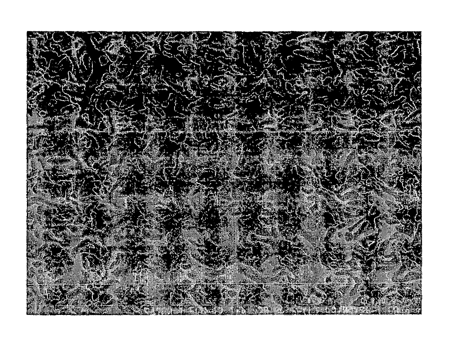
[0058]It was confirmed that a concave-convex structure was formed on the surface of the AlN underfilm, as shown in FIG. 1, and the surface roughness (average roughness Ra) of the flat region in the surface of the AlN underfilm was about 5 Å. Also, about 50% of the surface of the AlN film was occupied by the flat region. The FWHM in X-ray rocking curve of the (002) plane of the AlN underfilm was 80 seconds. The dislocation density of the GaN film was about 1×10⁷ / cm2.

Example

Example 3

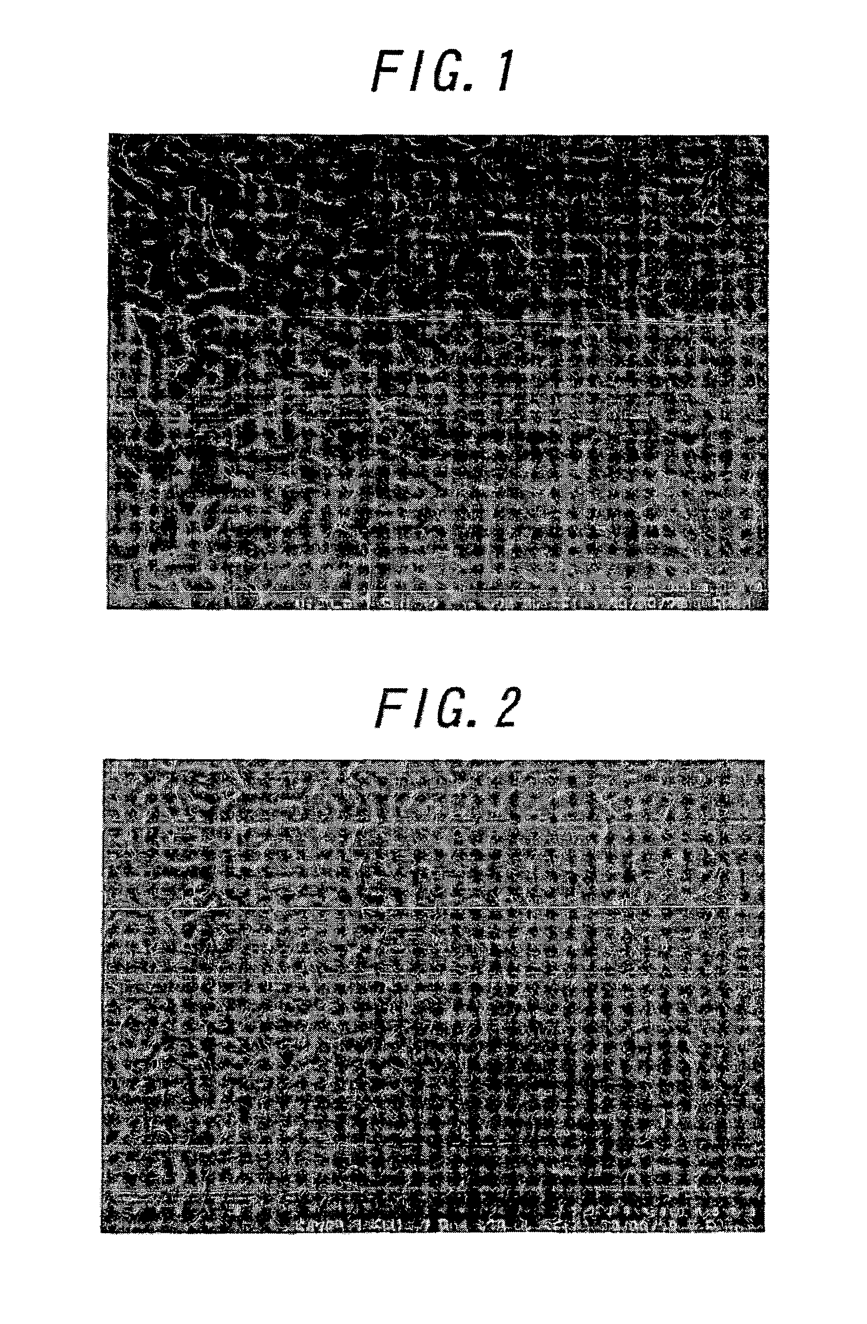
[0059]An AlN underfilm was formed in the same manner as Example 1, except that, in forming the second AlN film, the flow ratio NH3 / TMA was changed to 1500 from 1000.

[0060]FIG. 2 is a SEM photograph showing the surface configuration of the AlN underfilm. As is apparent from FIG. 2, about 20% of the surface of the AlN underfilm was occupied by the flat region. The FWHM in X-ray rocking curve of the (002) plane of the AlN underfilm was 80 seconds.

[0061]Then, a GaN film was formed in a thickness of 3 μm on the AlN underfilm in the same manner as Example 1. The dislocation density of the GaN film was found to be about 5×10⁶ / cm2 through TEM observation.


PUM

PropertyMeasurementUnit
Fractionaaaaaaaaaa
Fractionaaaaaaaaaa
Percent by atomaaaaaaaaaa

Abstract

A method for fabricating a Group III nitride film is provided, including the steps of preparing a substrate, forming an underfilm and then forming the Group III nitride film on the underfilm. The underfilm is a Group III nitride including at least 50 atomic percent of elemental Al for each of the Group III elements of the underfilm Group III nitride. The surface of the underfilm includes a contoured portion and a flat region, and less than 50% of the surface is occupied by the flat region.

Description

CROSS REFERENCE TO RELATED APPLICATION[0001]This application is a continuation of U.S. application Ser. No. 10 / 456,418, filed Jun. 6, 2003, now abandoned, which is a division of U.S. application Ser. No. 10 / 044,778, filed Nov. 7, 2001, now U.S. Pat. No. 6,649,493, the entireties of which are incorporated herein by reference.BACKGROUND OF THE INVENTION[0002](1) Field of the Invention[0003]This invention relates to a method for fabricating a Group III nitride film, an underlayer for fabricating a Group III nitride film and a method for fabricating the same underlayer, particularly usable for semiconductor films constituting a light-emitting diode or a high velocity IC chip.[0004](2) Related Art Statement[0005]Group III nitride films are employed as semiconductor films constituting light-emitting diodes, and recently, have received much attention as semiconductor films constituting high velocity IC chips for use in cellular phones.[0006]Such Group III nitride films are usually fabricat...

Claims


Application Information

Patent Timeline
IPC IPC(8): B32B9/00C23C16/02C23C16/30C30B25/18H01L21/20H01L21/205H01L33/12H01L33/16H01L33/22H01L33/32
CPCC23C16/0218C23C16/303C30B25/18H01L21/0237H01L21/0242H01L21/02658H01L21/02494H01L21/02502H01L21/02516H01L21/0254H01L21/0262H01L21/02458
Inventor ASAI, KEIICHIROSHIBATA, TOMOHIKONAKAMURA, YUKINORITANAKA, MITSUHIRO
Owner NGK INSULATORS LTD
Why Eureka
Try Eureka