AlN epitaxial layer and preparation method thereof

An epitaxial layer and isolation layer technology, applied in the field of AlN epitaxial layer and its preparation, can solve the problems of high density misfit dislocation, AlN surface cracking, device performance deterioration, etc., achieve rapid deposition, surface flattening, and reduce the concentration of point defects Effect

Active Publication Date: 2017-12-26
GUANGDONG INST OF SEMICON IND TECH
View PDF6 Cites 6 Cited by
  • Summary
  • Abstract
  • Description
  • Claims
  • Application Information

AI Technical Summary

Problems solved by technology

[0003] However, at this stage, there are still many problems in growing AlN on sapphire substrates. For example, the polarity control of the heterointerface is a great challenge to the epitaxy of the AlN template; Lead to AlN surface cracking and high density of misfit dislocations, etc., leading to serious deterioration of device performance

Method used


Image

  • AlN epitaxial layer and preparation method thereof

Examples


preparation example Construction

[0029] A method for preparing an AlN epitaxial layer provided in an embodiment of the present invention further includes:

[0030] S3. Deposit AlN on the nucleation layer at 1000-1100° C. to form a defect repair layer.

[0031] After creative work, the inventors found that if the rapid growth is performed directly at high temperature after the formation of the nucleation layer, the strain cannot be fully relaxed and threading dislocations can be effectively annihilated. Second, the inventors deposited a layer of defect repair layer on the nucleation layer before rapid growth. This defect repair layer can effectively reduce the concentration of point defects while ensuring strain release and dislocation annihilation, so as to provide future The high-temperature rapid growth process lays the foundation for obtaining higher-quality AlN epitaxial layers. The temperature range of 1000-1100° C. is the result of optimization by the inventors, and the effect of repairing defects in t...

Embodiment 1

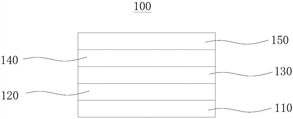
[0043] This embodiment provides an Al epitaxial layer 100 and its preparation method. The laminated structure of the Al epitaxial layer 100 is as follows: figure 1 As shown, the instrument used is Aixtron 3×2”FT CCS MOCVD, the substrate is a 2-inch (0001) sapphire substrate 110 with an offcut of 0.2 degrees on the c to m axis, the carrier gas is hydrogen, and the nitrogen source is ammonia , the organic aluminum source is TMAl.

[0044] S1. Introduce hydrogen gas, and bake the sapphire substrate 110 at 900° C. for 300 seconds under the condition that the reaction chamber pressure is 75 mbar.

[0045] The temperature of S2 is lowered to 650° C., and the pressure of the reaction chamber is 50 mbar, and TMAl2s is pre-spread, and the source flow rate is 22 sccm.

[0046] S3. Growing a 2nm N-polar isolation layer 120 on the sapphire substrate 110 at 650° C. and a reaction chamber pressure of 50 mbar. Wherein, the molar flow ratio of ammonia gas and TMAl is 50.

[0047] S4. Raise...

Embodiment 2

[0052] This embodiment provides a kind of Al epitaxial layer and preparation method thereof, the instrument adopted is Aixtron 3 * 2 " FTCCS MOCVD, the substrate is the 2-inch (0001) plane sapphire substrate whose offcut is c to m axis 0.2 degree, The carrier gas is hydrogen, the nitrogen source is ammonia, and the organic aluminum source is TMAl.

[0053] S1. Introduce hydrogen gas, and bake the sapphire substrate at 930° C. for 200 seconds under the condition that the reaction chamber pressure is 100 mbar.

[0054] The temperature of S2 is lowered to 650°C, and the pressure of the reaction chamber is 50mbar, pre-spreading TMAl5s, and the source flow rate is 15sccm.

[0055] S3. At 650° C. and the pressure of the reaction chamber at 50 mbar, a 5 nm N polarity isolation layer is grown. Wherein, the molar flow ratio of ammonia gas and TMAl is 35.

[0056] S4. Raise the temperature to 930° C. and grow a 40 nm nucleation layer under the condition that the reaction chamber press...


PUM


Abstract

An AlN epitaxial layer and preparation method thereof relate to the field of semiconductor epitaxy technology. According to the invention, an N polarity isolation layer grows at a comparatively low temperature, so that the N polarity is isolated well and single Al polarity is formed. Then a nucleating layer is formed on the N-polarity isolation layer at a medium temperature. The surface transfer ability of Al atoms at the medium temperature is improved and the quality of the nucleating layer is improved. The temperature is increased further and a defect repairing layer is settled on the nucleating layer at a comparatively high temperature, so that spot defect concentration can be reduced in a condition with stress release and dislocation annihilation. Finally, the temperature is increased continually and the high transfer ability of the Al atoms is kept at a high temperature, so that quick settlement on the basis of the defect repairing layer is realized and the growth efficiency is improved. The preparation method provided by the invention is simple in technique, convenient to operate and provides high growth efficiency. The AlN epitaxial layer prepared by adopting the preparation method has characteristics of smooth surface, single Al polarity and low dislocation annihilation.

Description

technical field [0001] The invention relates to the technical field of semiconductor epitaxy, in particular to an AlN epitaxial layer and a preparation method thereof. Background technique [0002] In recent years, due to many advantages such as direct bandgap, adjustable bandgap, high temperature resistance, and radiation resistance, AlGaN materials have shown broad application prospects in the fields of optoelectronic devices and electronic devices. From the perspective of growth strain and light transmittance, in order to prepare high-quality AlGaN materials and related devices, the use of AlN homogeneous substrates and AlN / sapphire template substrates is an ideal choice. In the existing technology, due to the lack of low-cost, high-quality, and large-size AlN single crystal substrates, compared with AlN homogeneous substrates, growing AlN templates on cheap and mature sapphire substrates is the mainstream technology in this field route. [0003] However, at this stage,...

Claims


Application Information

Patent Timeline
Patent Type & Authority Applications(China)
IPC IPC(8): H01L21/205
CPCH01L21/02414H01L21/02458H01L21/0254H01L21/0262
Inventor 何晨光赵维吴华龙张康贺龙飞陈志涛
Owner GUANGDONG INST OF SEMICON IND TECH
Why Eureka
Try Eureka