Semiconductor device and manufacturing method thereof

a semiconductor and manufacturing method technology, applied in the direction of transistors, electroluminescent light sources, electric lighting sources, etc., can solve the problems of display unevenness, signal delay due to resistance of wiring, and risk of luminance variation on display screens, etc., to achieve sufficient reliability and easy manufacturing process

Active Publication Date: 2010-07-01
SEMICON ENERGY LAB CO LTD
View PDF100 Cites 35 Cited by
  • Summary
  • Abstract
  • Description
  • Claims
  • Application Information

AI Technical Summary

Benefits of technology

[0028]For a thin film transistor in which a channel formation region is formed using a semiconductor film

Problems solved by technology

In particular, when a display device with a large-area display is manufactured, a problem of signal delay due to resistance of a wiring becomes prominent.
Moreover, in a liquid crystal display device or a display device including an organic light-emitting element, for example, in the case where the semiconductor device has large variation in transistor characteristics, there is a risk that display unevenness occurs due to the variation.
In particular, in a display device including a light-emitting element, in the case where there is large variation in ON current (Ion) of TFTs (TFTs supplying current

Method used


Image

  • Semiconductor device and manufacturing method thereof
  • Semiconductor device and manufacturing method thereof
  • Semiconductor device and manufacturing method thereof

Examples


embodiment 1

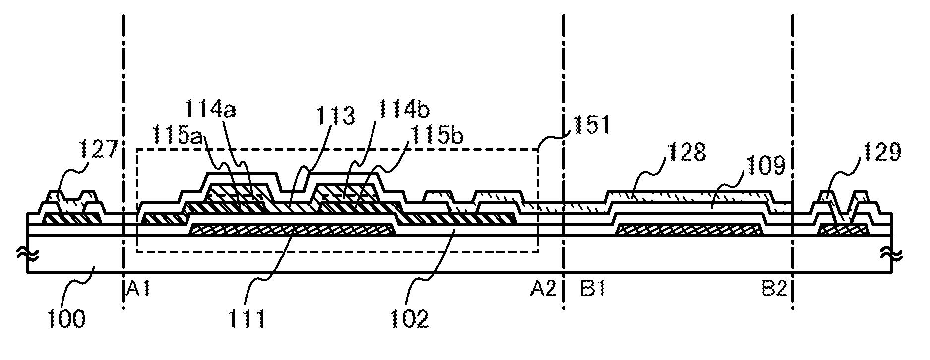
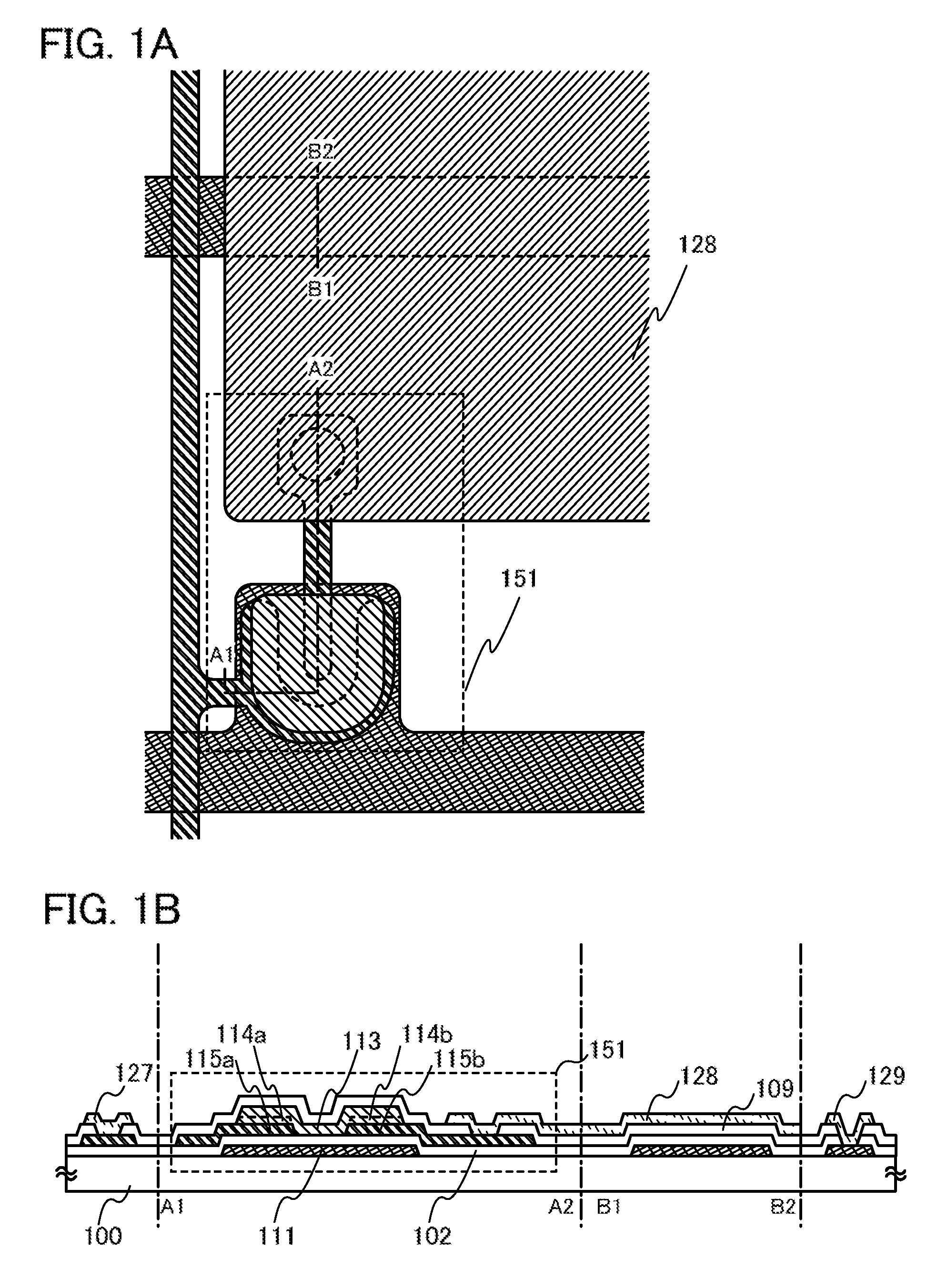
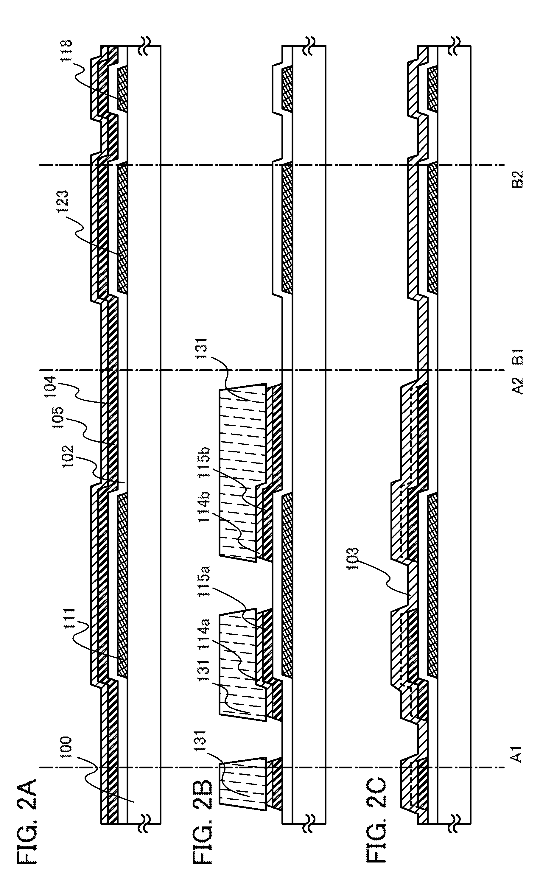
[0077]Embodiment 1 describes a thin film transistor as an example of a semiconductor device, and a manufacturing process thereof. In specific, a process for manufacturing a pixel portion of a display device including a thin film transistor is described.

[0078]FIGS. 1A and 1B illustrate a thin film transistor of Embodiment 1. FIG. 1A is a plan view and FIG. 1B is a cross-sectional view taken along lines A1-A2 and B1-B2 in FIG. 1A.

[0079]In a thin film transistor 151 illustrated in FIGS. 1A and 1B, a gate electrode layer 111 is formed over a substrate 100, a gate insulating film 102 is formed over the gate electrode layer 111, and a first electrode layer 115a and a second electrode layer 115b serving as a source electrode layer and a drain electrode layer are formed over the gate insulating film 102 so that end portions of the first electrode layer 115a and the second electrode layer 115b overlap with the gate electrode layer 111. A first oxide semiconductor layer 113 is provided so as ...

embodiment 2

[0126]In Embodiment 2, an embodiment of the present invention is described below based on an example in which an inverter circuit is formed using two n-channel thin film transistors.

[0127]A driver circuit for driving a pixel portion of a board for an active matrix display device is formed using an inverter circuit, a capacitor, a resistor, and the like. When two n-channel TFTs are combined to form an inverter circuit, there are two types of combinations: a combination of an enhancement type transistor and a depletion type transistor (hereinafter, a circuit formed by such a combination is referred to as an “EDMOS circuit”) and a combination of enhancement type TFTs (hereinafter, a circuit formed by such a combination is referred to as an “EEMOS circuit”). Note that when the threshold voltage of the n-channel TFT is positive, the n-channel TFT is defined as an enhancement type transistor, while when the threshold voltage of the n-channel TFT is negative, the n-channel TFT is defined a...

embodiment 3

[0148]Embodiment 3 describes a thin film transistor of a semiconductor device. Specifically, a pixel portion of a display device including a top-gate thin film transistor is described.

[0149]FIGS. 6A and 6B illustrate a thin film transistor of Embodiment 3. FIG. 6A is a plan view, and FIG. 6B is a cross-sectional view taken along lines A1-A2 and B1-B2 of FIG. 6A.

[0150]In a thin film transistor 154 illustrated in FIGS. 6A and 6B, a first electrode layer 115a and a second electrode layer 115b serving as a source electrode layer and a drain electrode layer are formed over a substrate 100, a first protective layer 114a is formed over the first electrode layer 115a, and a second protective layer 114b is formed over the second electrode layer 115b. A first semiconductor layer 113 is formed so as to be in contact with side face portions of the first electrode layer 115a and the second electrode layer 115b and side face portions and top face portions of the first protective layer 114a and th...


PUM


Abstract

One of factors that increase the contact resistance at the interface between a first semiconductor layer where a channel is formed and source and drain electrode layers is a film with high electric resistance formed by dust or impurity contamination of a surface of a metal material serving as the source and drain electrode layers. As a solution, a first protective layer and a second protective layer including a second semiconductor having a conductivity that is less than or equal to that of the first semiconductor layer is stacked successively over source and drain electrode layers without exposed to air, the stack of films is used for the source and drain electrode layers.

Description

BACKGROUND OF THE INVENTION[0001]1. Field of the Invention[0002]The present invention relates to a semiconductor device and a manufacturing method thereof. For example, the present invention relates to a thin film transistor or a semiconductor device including an oxide semiconductor film in a channel formation region. Moreover, the present invention relates to, for example, an electro-optic device typified by a liquid crystal display panel including a thin film transistor or to a light-emitting display device including a thin film transistor and an organic light-emitting element. Furthermore, the present invention relates to an electronic appliance in which such an electro-optic device or a light-emitting display device as above is incorporated as a component.[0003]The semiconductor device in this specification refers to all devices that can function by utilizing semiconductor characteristics; semiconductor elements, electro-optic devices, semiconductor circuits, and electronic appl...

Claims


Application Information

Patent Timeline
IPC IPC(8): H01L29/786H01L21/336H01L29/12H05B44/00
CPCH01L29/78606H01L29/78618H01L29/7869H01L33/0041H01L2924/0002H01L29/66969H01L2924/00H01L29/45H01L29/66742
Inventor AKIMOTO, KENGOTSUBUKU, MASASHI
Owner SEMICON ENERGY LAB CO LTD
Why Eureka
Try Eureka