
Lensless optical navigation device for directing radiation via reflection by three total internal surfaces
a technology of optical navigation and reflection, applied in the direction of electrical instruments, electric digital data processing, electrical equipment, etc., can solve the problems of pattern formation on the imaging surface, and achieve the effects of convenient assembly, faster and simpler device manufacturing, and convenient assembly of optical navigation devices
- Summary
- Abstract
- Description
- Claims
- Application Information
AI Technical Summary
Benefits of technology
Problems solved by technology
Method used
Image

Examples
Embodiment Construction
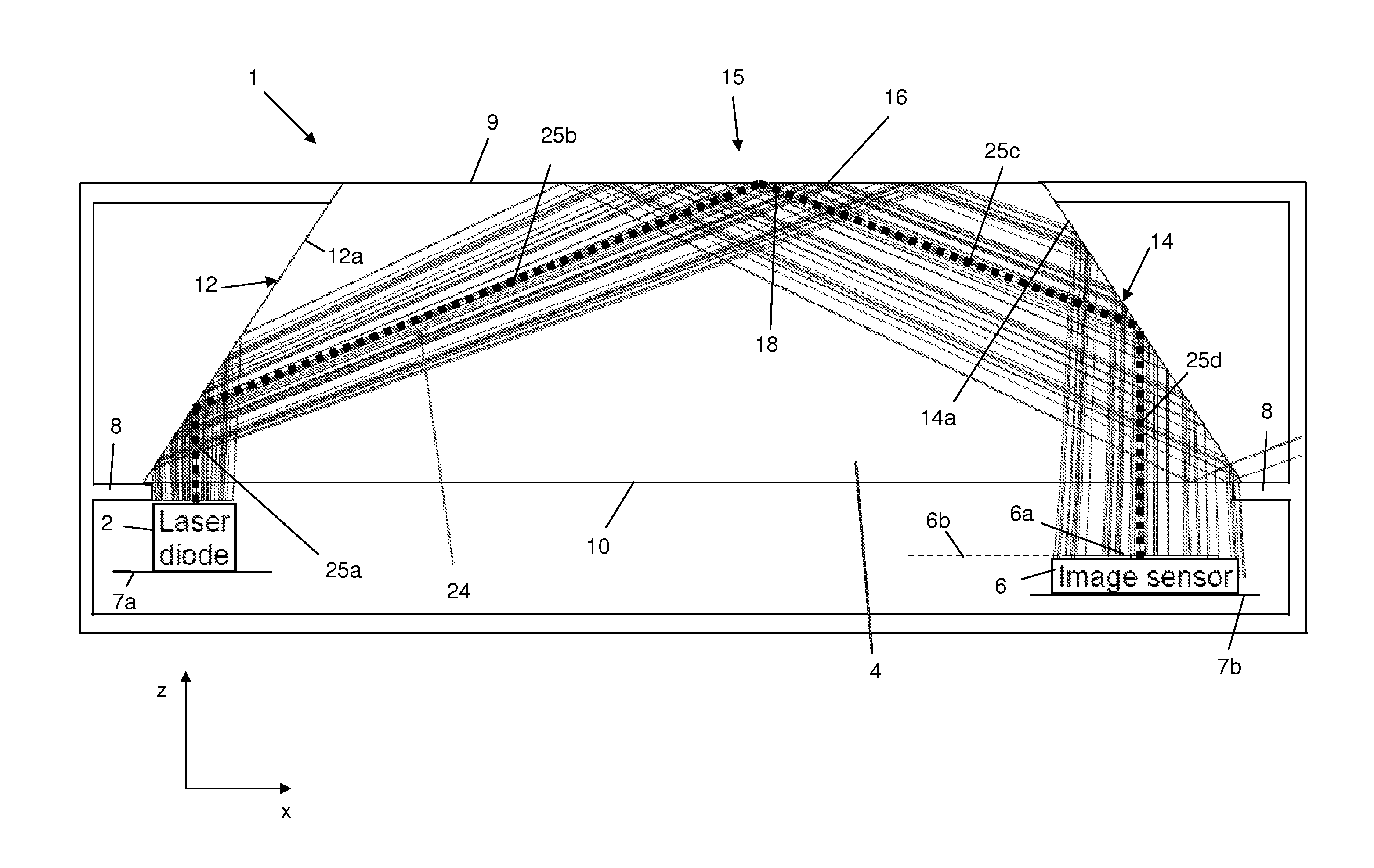
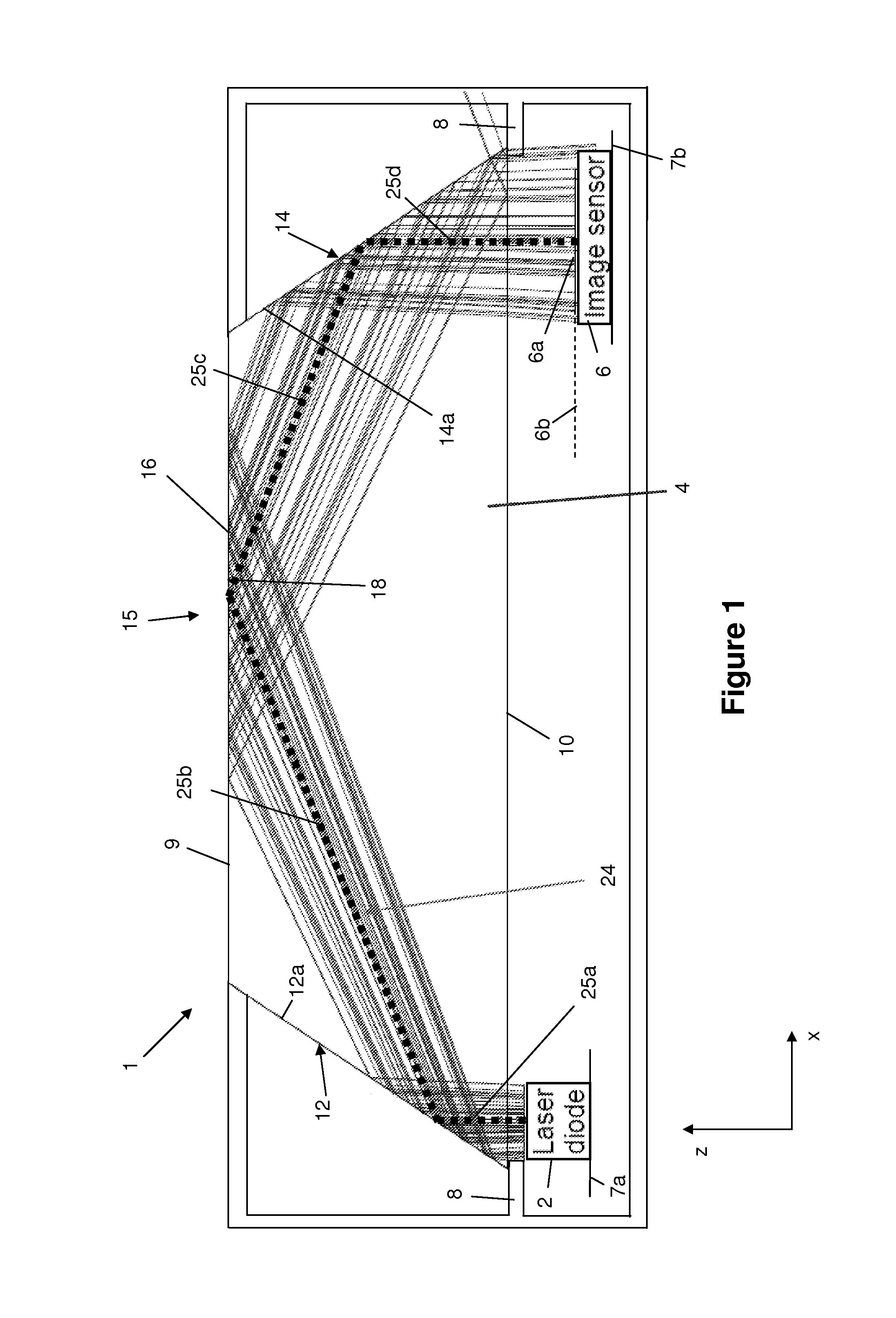
[0049]FIG. 1 is a schematic cross sectional view of an optical navigation device 1 comprising a laser diode 2 (typically a VCSEL but may be any other suitable type of laser diode), an optical element 4 and an image sensor 6 having a substantially planar imaging surface 6a lying on an imaging plane 6b. The laser diode 2 and image sensor 6 are mounted on separate circuit boards 7a, 7b, while the optical element 4 is suspended above the circuit boards 7a, 7b by a supportive housing 8. It will be understood that the laser 2 and image sensor 6 may alternatively be mounted on the same circuit board.
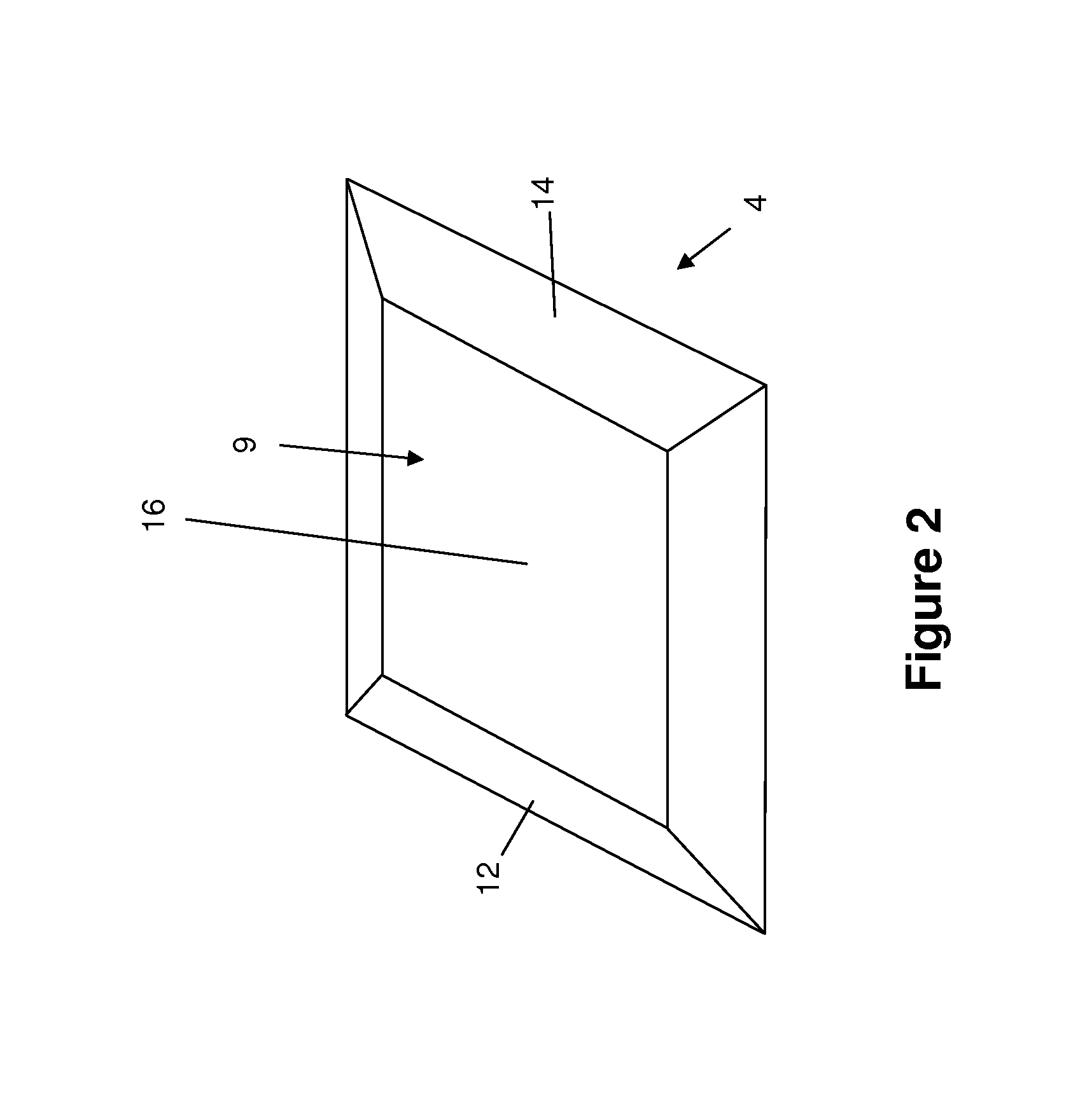
[0050]As shown in FIGS. 1 and 2, the optical element 4 comprises an upper, user input face 9 and a lower face 10 with a pair of angled side faces 12, 14 extending between them, the side faces 12, 14 converging towards each other as they extend from the lower face 10 to the upper face 9. A touch sensitive input area 15 is formed at an intermediate region of the user input face 9 between the angl...
PUM
 Abstract
Description
Claims
Application Information