
Methods for forming vertical and sharp junctions in finFET structures

a technology of finfets and vertical joints, applied in the direction of basic electric elements, electrical apparatus, semiconductor devices, etc., can solve the problem of device threshold variability on the same substrate, and achieve the effect of improving device performance, shortening channel lengths, and increasing effective curren

Active Publication Date: 2015-12-01
IBM CORP +2
View PDF3 Cites 37 Cited by
  • Summary
  • Abstract
  • Description
  • Claims
  • Application Information

AI Technical Summary

Benefits of technology

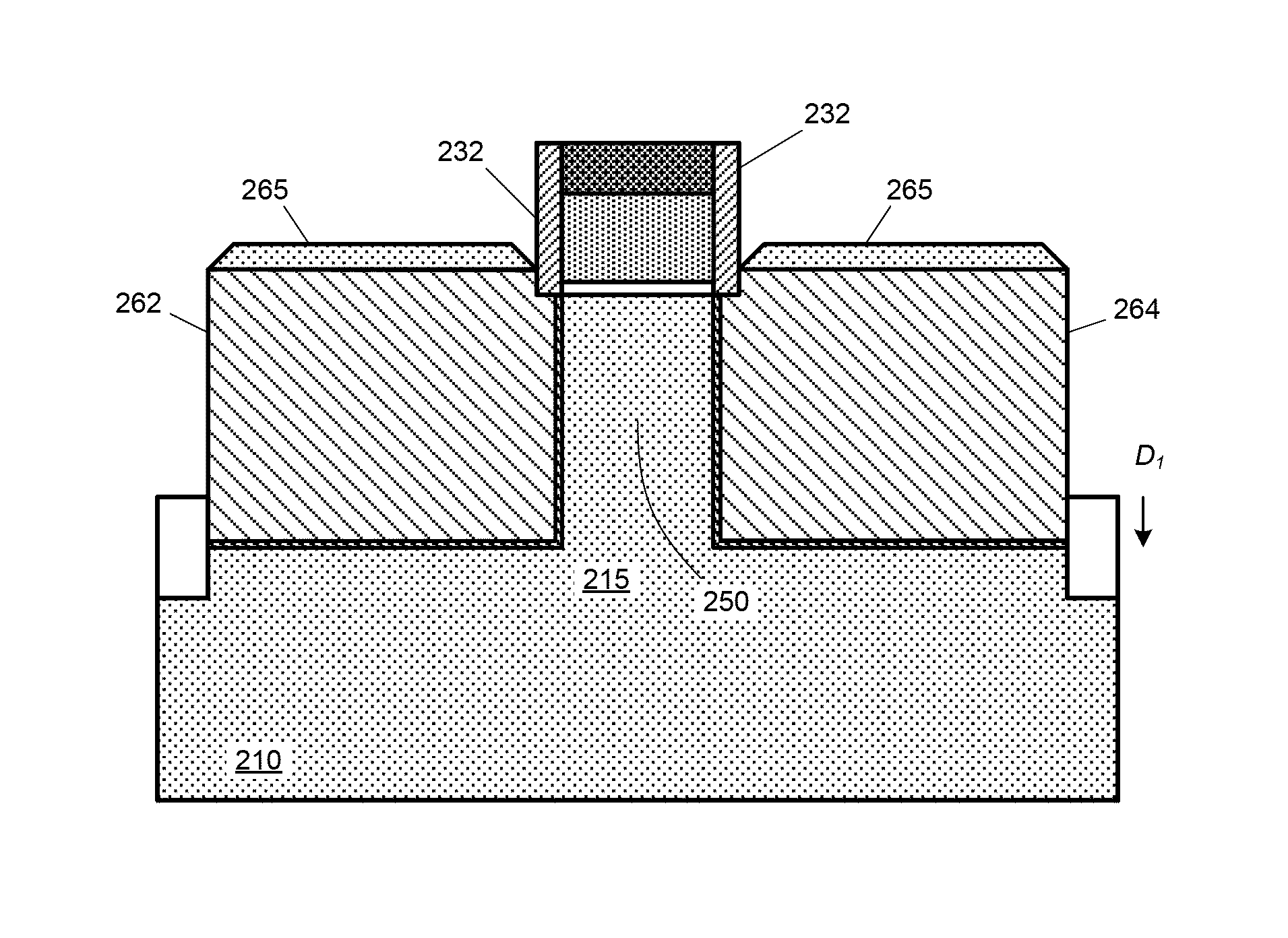
This patent describes a way to make the junctions between the source and drain of finFETs vertical and sharp. This can improve device performance by making the junctions faster and more effective. The method involves using a buffer made of a special dopant material that is deposited on recessed source and drain structures. This buffer creates raised source and drain structures that help to strain the channel region of the finFET. The result is better performance without needing a thermal diffusion step to drive in the dopants.

Problems solved by technology

Such tapered junction profiles can undesirably lead to device threshold variability on a same substrate.

Method used


Image

  • Methods for forming vertical and sharp junctions in finFET structures
  • Methods for forming vertical and sharp junctions in finFET structures
  • Methods for forming vertical and sharp junctions in finFET structures

Examples


Embodiment Construction

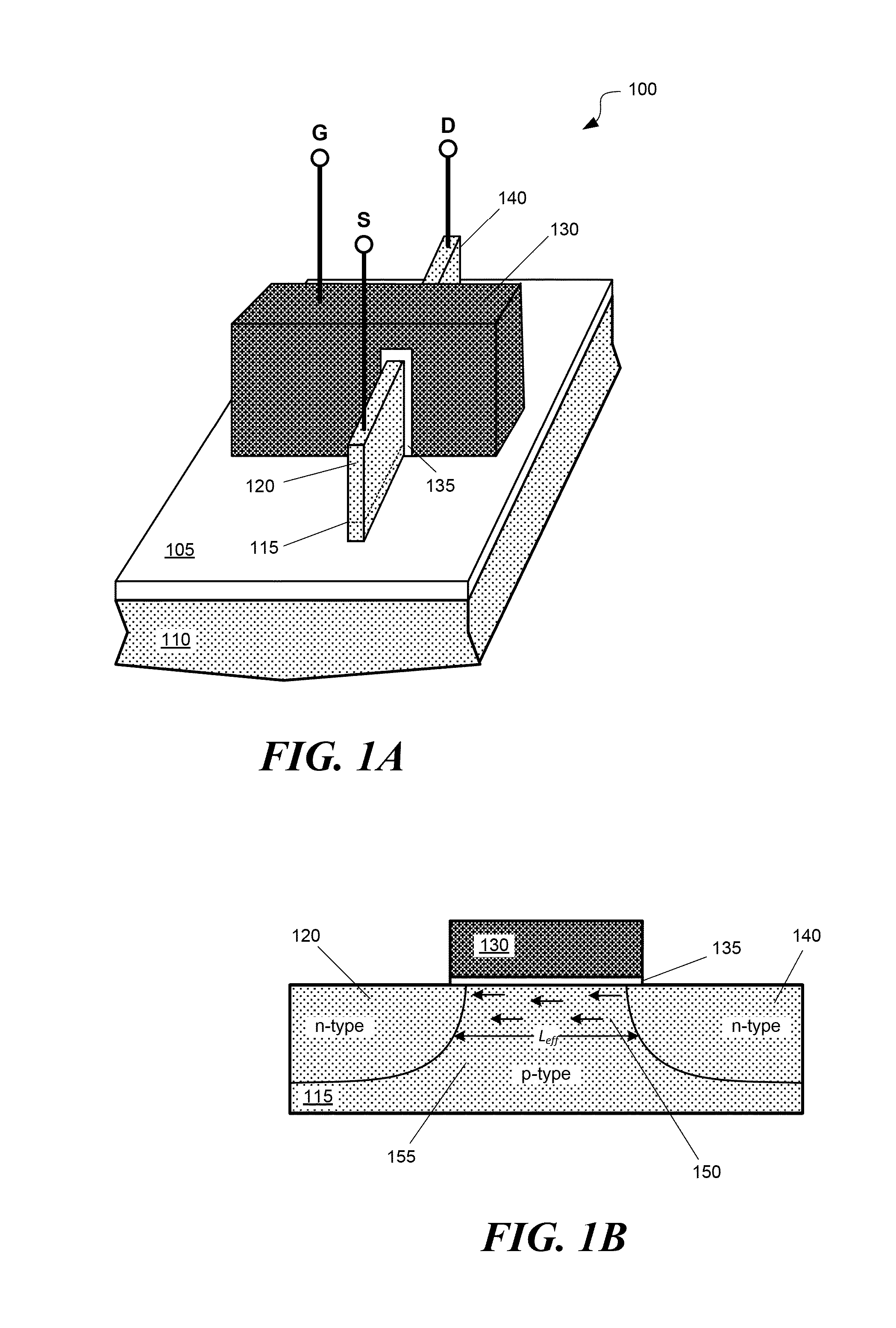
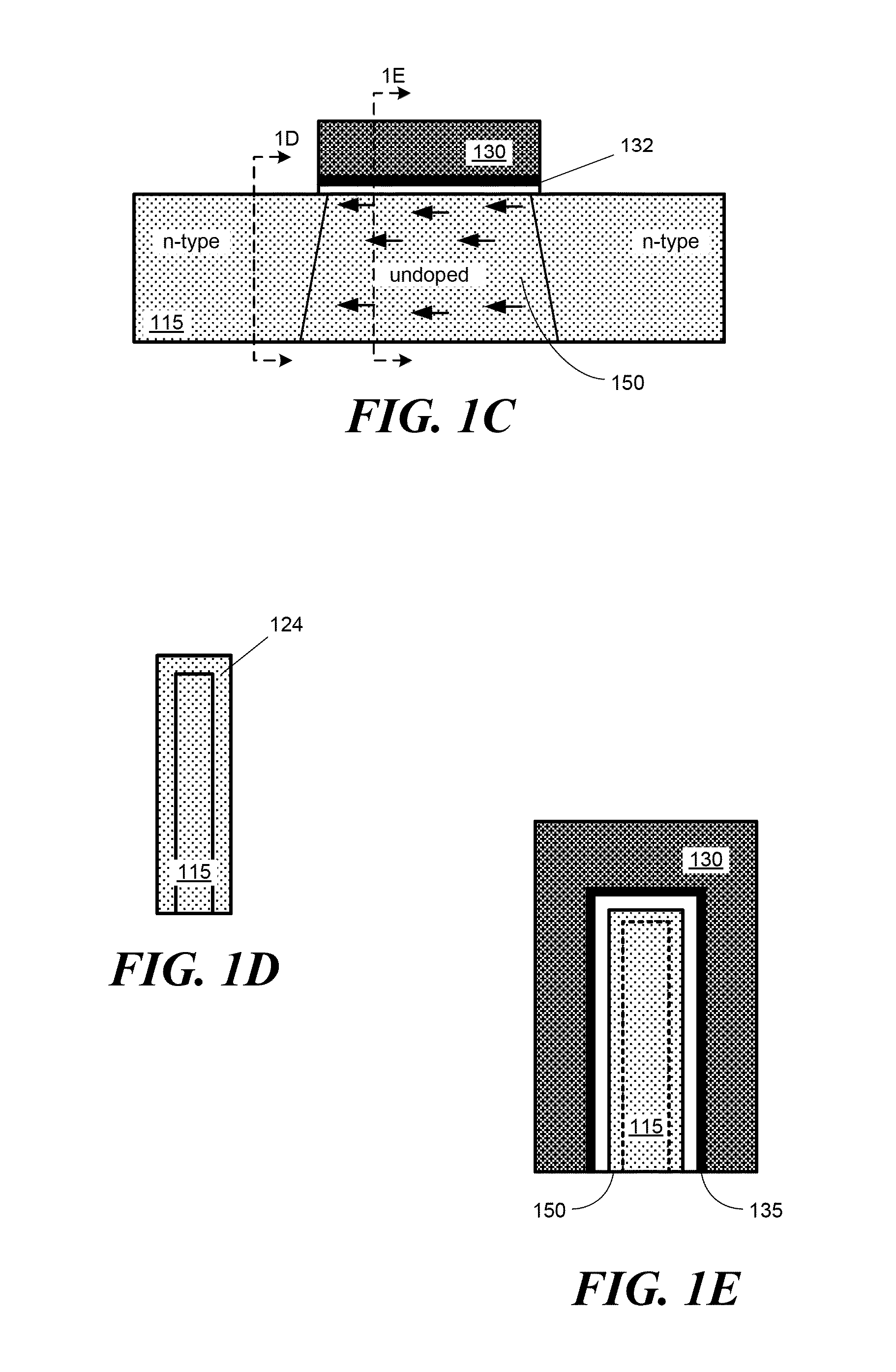
[0033]An example of a finFET 100 is depicted in the perspective view of FIG. 1A. A finFET may be fabricated on a bulk semiconductor substrate 110, e.g., a silicon substrate, and comprise a fin-like structure 115 that runs in a length direction along a surface of the substrate and extends in a height direction normal to the substrate surface. The fin 115 may have a narrow width, e.g., less than 50 nanometers. There may be an electrically-insulating layer 105, e.g., an oxide layer, on a surface of the substrate 110. The fin may pass through the insulating layer 105, but be attached to the semiconducting substrate 110 at a lower region of the fin. A gate structure comprising a conductive gate material 130 (e.g., polysilicon, metal, or a metal silicide) and a gate insulator 135 (e.g., an oxide or high-k dielectric) may be formed over a region of the fin. The finFET may further include a source region 120 and drain region 140 adjacent to the gate. A finFET may also include integrated sou...


PUM


Abstract

Methods and structures for forming short-channel finFETs with vertical and abrupt source and drain junctions are described. During fabrication, source and drain regions of the finFET may be recessed vertically and laterally under gate spacers. A buffer having a high dopant density may be formed on vertical sidewalls of the channel region after recessing the fin. Raised source and drain structures may be formed at the recessed source and drain regions. The raised source and drain structures may impart strain to the channel region.

Description

BACKGROUND[0001]1. Technical Field[0002]The technology relates to methods and structures for making finFETs having vertical and abrupt source and drain junctions.[0003]2. Discussion of the Related Art[0004]Transistors are fundamental device elements of modern digital processors and memory devices, and have found numerous applications in various areas of electronics including data processing, data storage, and high-power applications. Currently, there are a variety of transistor types and designs that may be used for different applications. Various transistor types include, for example, bipolar junction transistors (BJT), junction field-effect transistors (JFET), metal-oxide-semiconductor field-effect transistors (MOSFET), vertical channel or trench field-effect transistors, and superjunction or multi-drain transistors.[0005]Two types of transistors have emerged within the MOSFET family of transistors that show promise for scaling to ultra-high density and nanometer-scale channel len...

Claims


Application Information

Patent Timeline
IPC IPC(8): H01L29/78H01L29/66
CPCH01L29/785H01L29/66553H01L29/66795H01L29/7848
Inventor LIU, QINGYEH, CHUN-CHENXIE, RUILONGCAI, XIUYU
Owner IBM CORP
Learn More