Semiconductor storage device with two control lines
a technology of semiconductor devices and storage devices, applied in semiconductor devices, digital storage, instruments, etc., can solve the problems of not yet being made into a product, inability to use in frequent rewriting, large power consumption of storing data during standby, etc., to achieve small leakage current, reduce power consumption associated with storing data, and keep stably
- Summary
- Abstract
- Description
- Claims
- Application Information
AI Technical Summary
Benefits of technology
Problems solved by technology
Method used
Image

Examples
embodiment 1
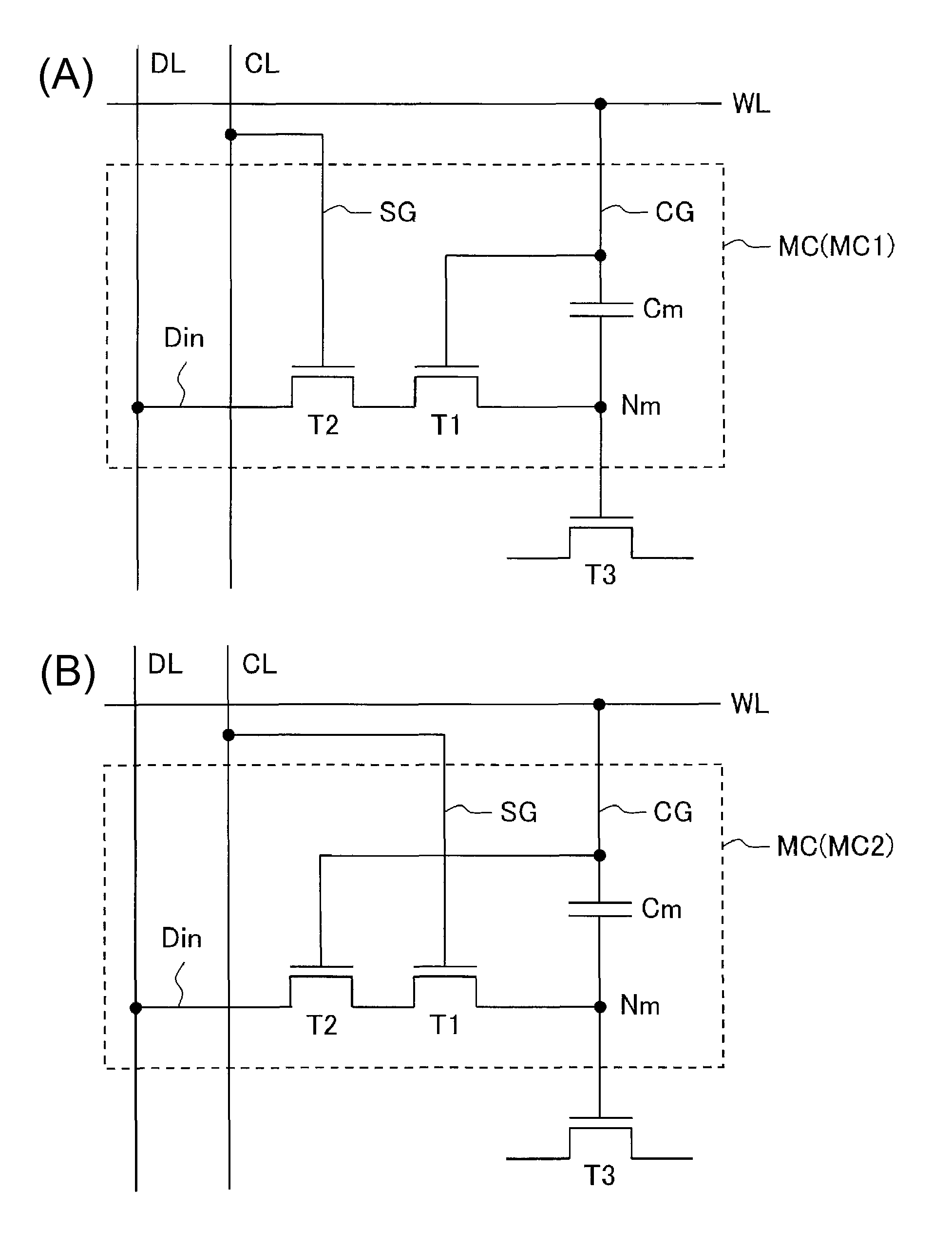
[0027]In Embodiment 1, the circuit configuration of a memory cell and the writing operation of data in the semiconductor storage device (hereinafter, “storage device”) of the present invention will be described.
[0028]FIGS. 1(A) and 1(B) show an equivalent circuit diagram of two types of memory cells MC (MC1, MC2). Both types of memory cells MC have a first transistor T1 that is an oxide semiconductor insulated-gate FET, a second transistor T2 that is an oxide semiconductor insulated-gate FET, and a capacitor Cm.
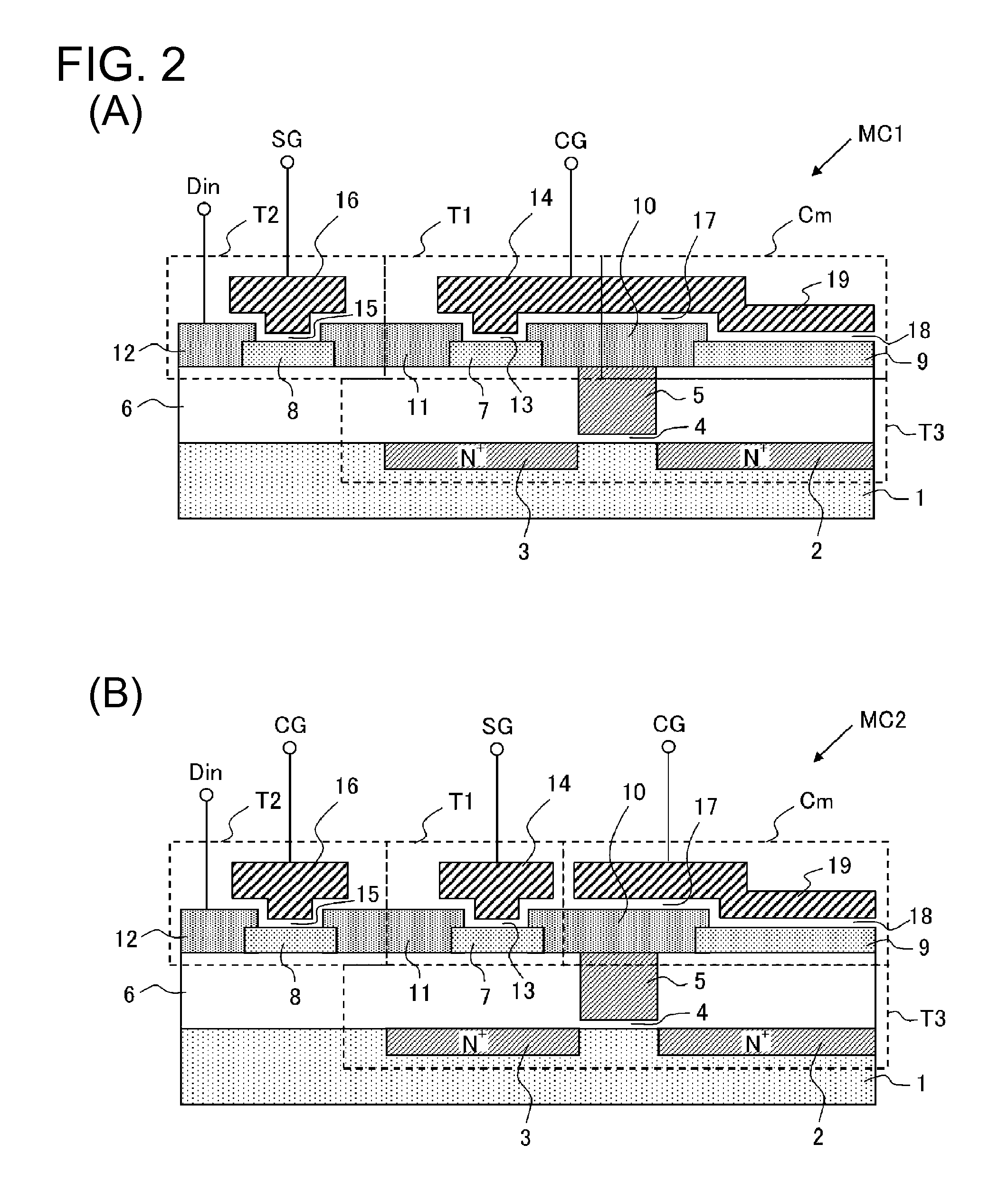
[0029]As shown in FIGS. 1(A) and 1(B), in each memory cell MC, a storage node NM is formed of a source of a first transistor T1 and an end of a capacitor Cm connected thereto, the drain of the first transistor T1 being connected to the source of the second transistor T2, the drain of the second transistor T2 being connected to the data input terminal Din. Also, as shown in FIG. 2, the first and second transistors T1 and T2 have a structure in which the drain and source are in...
embodiment 2
[0045]The circuit configuration and the circuit operation for a non-volatile random-access memory (hereinafter, NVRAM) constituted of the memory cell MC described in Embodiment 1 will be described. Embodiment 2 is described with the first type memory cell MC1 as an example of a memory cell MC. Even if a second type memory cell MC2 is used, the writing operation for the memory cell MC is the same as for the first type memory cell MC1, and thus, the operation of the NVRAM is also essentially the same as the first type memory cell MC1.
[0046]FIG. 3 shows an equivalent circuit diagram of an NVRAM memory cell array MA3. The memory cell array MA3 is configured by aligning a plurality of the memory cells MC and a plurality of memory cells MC3 including the third transistors T3 in a matrix in the row direction and in the column direction. In Embodiment 2, one third transistor T3 is provided for each memory cell MC3 as a reading transistor for the data stored in the storage node Nm. In FIG. 3...
embodiment 3
[0057]A logic device including a field programmable gate array (FPGA), a programmable logic device (PLD), or the like that is constituted of the memory cell MC described in Embodiment 1 and that has a reconfigurable logic circuit will be schematically described.
[0058]In Embodiment 3, a memory cell array MA that is formed by arranging a plurality of memory cells MC (MC1 or MC2) described in Embodiment 1 in a matrix is used as a configuration memory that stores data defining the logical structure of a reconfigurable logic circuit. Then, a third memory cell element T3 having a gate to which a storage node Nm of each memory cell MC is connected is used as a transistor that functions as a switch that switches the logical structure mentioned above.
[0059]In FIG. 5, an equivalent circuit diagram of the memory cell array MA used as the above-mentioned configuration memory is shown. In Embodiment 3, in a manner similar to the memory cell MC, a plurality of the third transistors T3 are also ar...
PUM
 Abstract
Description
Claims
Application Information