Differential bit cell

a differential bit cell and memory cell technology, applied in the field of memory devices, can solve the problems of variances that tend to negatively affect the performance of memory cells, memory devices are becoming more dense, and may introduce various process variations, so as to reduce the mismatch effect of transistors and improve the performance of memory devices

Active Publication Date: 2015-12-22
AVAGO TECH INT SALES PTE LTD
View PDF2 Cites 0 Cited by
  • Summary
  • Abstract
  • Description
  • Claims
  • Application Information

AI Technical Summary

Benefits of technology

[0007]Methods, systems, and apparatuses are described for reducing the mismatch effects of transistors that are caused by process variations and improving the performance of a memory device, substantially as shown in and / or described herein in connection with at least one of the figures, as set forth more completely in the claims.

Problems solved by technology

In other words, memory devices have been becoming denser.
One problem that arises when manufacturing relatively smaller transistors is that various process variations may be introduced.
Such variances tend to negatively affect the performance of the memory cells.

Method used


Image

  • Differential bit cell
  • Differential bit cell
  • Differential bit cell

Examples


example embodiments

II. Example Embodiments

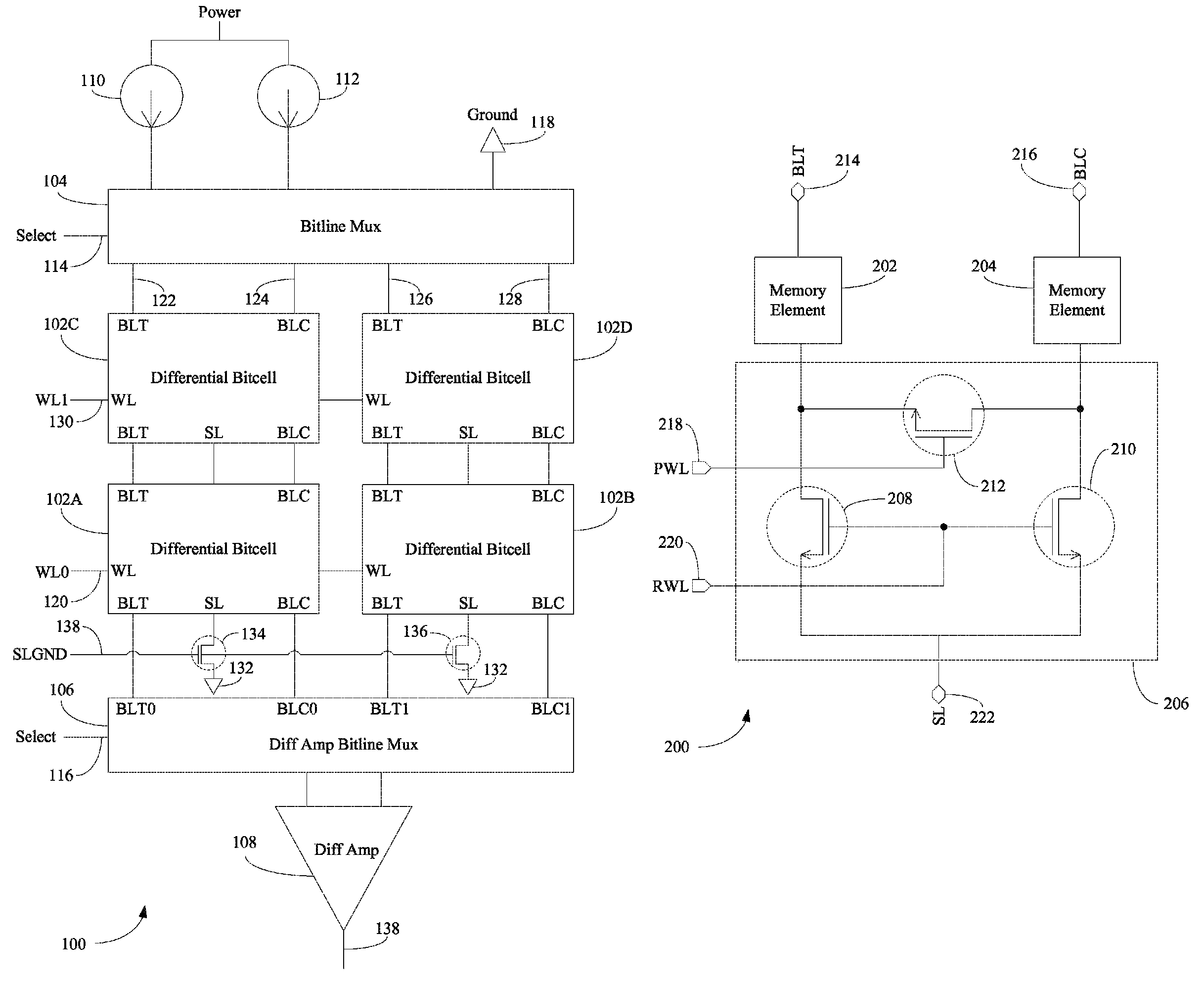
[0020]FIG. 1 is block diagram of an example memory device 100 in accordance with an embodiment. As shown in FIG. 1, memory device 100 includes differential bit cells 102A-102D, a bitline multiplexor (mux) 104, a differential amplifier (diff amp) bitline mux 106, a diff amp 108, a first current source 110, and a second current source 112. In the illustrated exemplary embodiment, memory device 100 includes four differential bit cells 102A-102D arranged into two rows and two columns (i.e., a 2×2 configuration) for illustrative purposes, though persons skilled in the relevant art(s) will appreciate that additional or fewer differential bit cells and / or additional or fewer rows and / or columns may be employed without departing from the spirit and scope of the present embodiments.

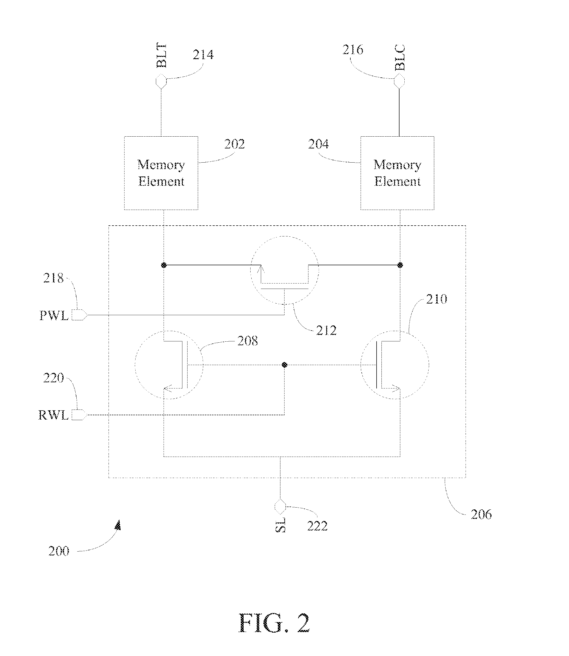
[0021]As will be described below with reference to FIG. 2, each of differential bit cells 102A-102D may include two memory elements. Each of the two memory elements includes an associated ac...


PUM


Abstract

A differential bit cell includes two memory elements that are configured to have different states. Each of the two memory elements is connected to a respective switching element. Each of these switching elements may have process variances, which may result in a degradation of read and / or write margins. To mitigate the effect of such variances, another switching element is coupled to the two memory elements and their respective switching elements in a manner that couples the aforementioned switching elements in a parallel fashion. In this way, the mismatch effects between the switching elements can be negated during read operations. During programming operations, such a configuration allows for the programming of both memory elements to different states with a single current pulse and also reduces the effective resistance of the programming path.

Description

CROSS-REFERENCE TO RELATED APPLICATION(S)[0001]This application claims the benefit of U.S. Provisional Application No. 61 / 837,033, filed Jun. 19, 2013, the entirety of which is incorporated by reference herein.BACKGROUND[0002]1. Technical Field[0003]The subject matter described herein relates to memory devices. In particular, the subject matter described herein relates to memory devices having different resistive states.[0004]2. Description of Related Art[0005]The basic unit of a semiconductor memory is a memory cell. A memory cell is capable of storing a single bit of information. Industry trends continuously demand for smaller, faster, and higher capacity memories. Accordingly, the memory cell has steadily shrunk in size to enable more and more cells per unit area. In other words, memory devices have been becoming denser.[0006]Typically, memory cells include one or two transistors. Accordingly, as memory cells decrease in size, so do the transistor(s). One problem that arises when...

Claims


Application Information

Patent Timeline
Patent Type & Authority Patents(United States)
IPC IPC(8): G11C11/00G11C13/00
CPCG11C13/0069G11C13/0002G11C13/004G11C2013/0057G11C2013/0042
Inventor HYNES, OWENSCHMITT, JONATHAN
Owner AVAGO TECH INT SALES PTE LTD
Why Eureka
Try Eureka