2D programmable aperture mechanism

a technology of aperture mechanism and programmable aperture, which is applied in the field of optical inspection systems and methods, can solve the problems of limited number of aperture shapes and sizes, and limited number of shapes that can be presented by the tape drive mechanism, so as to reduce the amount of heat accumulated by the mechanical pixel element, reduce the number of mechanical pixel elements, and avoid excessive heat accumulation in each mechanical pixel

Active Publication Date: 2016-02-09
KLA CORP
View PDF12 Cites 18 Cited by
  • Summary
  • Abstract
  • Description
  • Claims
  • Application Information

AI Technical Summary

Benefits of technology

[0018]Each mechanical pixel includes a surface that may be exposed to incoming light. In some embodiments, the surface is highly absorptive, or treated with a highly absorptive coating, to absorb incoming light. In this manner, light that is blocked by the mechanical pixel is absorbed and stray reflections that may interfere with the performance of the optical inspection system are minimized. To dissipate heat accumulated by the mechanical pixel element, a cooling system such as forced air cooling, liquid immersion, or radiative cooling may be employed. In some other embodiments, the surface is highly reflective to avoid excessive heat accumulation in each mechanical pixel. In some of these embodiments, the surface is tilted such that the normal to the surface is not aligned with the beam of incoming light. In this manner, light reflected from the surface is directed away from the beam of light passing through the programmable aperture.
[0019]In some embodiments, each mechanical pixel includes one or more protrusion features configured to overlap with complementary features located adjacent mechanical pixels. In combination, these complementary features create a light trap that prevents the transmission of light through any nominal gap between pixels.
[0020]In some embodiments, the linear guiding elements are wire elements stretched across the aperture area. The cross-section of the wire elements may be rectangular in shape to constrain the position of each mechanical pixel in five degrees of freedom while presenting a small cross-sectional area exposed to the incoming beam of light. In some other embodiments, a wire element with a T-shaped cross-section may be employed to prevent incoming light from grazing the side of the wire element.

Problems solved by technology

However, the number of aperture shapes and sizes is limited by the number of predetermined apertures available on a particular wheel.
Again, the number of aperture shapes and sizes is limited by the number of predetermined apertures available on a particular linear slider.
Similarly, the number of shapes that can be presented by the tape drive mechanism is limited by the number of predetermined apertures available on the particular tape.
However, liquid crystal arrays suffer from a number of practical limitations.
Firstly, liquid crystal array pixels are not fully transmissive when programmed in a transmissive mode.
This leads to excessive light loss.
This is particularly costly in the context of a modern inspection system.
Secondly, liquid crystal array pixels are not fully occluding in a blocking mode.
This leads to excessive light leakage that is detrimental in a modern optical inspection system.
Moreover, liquid crystal arrays may also induce stray light, scattered light, and optical aberrations that further degrade optical inspection performance.
Furthermore, liquid crystal arrays may also suffer from limited lifetime when exposed to short wavelength light, particularly at high power densities.
However, tilt mirror arrays also suffer from light loss and optical artifacts such as stray light, scattered light, and optical aberrations that limit optical inspection system performance.
However, photofilm systems, are not completely transmissive and completely occlusive, leading to undesirable light loss and light leakage.
Moreover, exposure and development of photofilms is costly and time consuming, and the resulting films have a low damage threshold.
Photofilm systems may also cause contamination of other elements of UV, DUV, and VUV light systems commonly employed in modern inspection systems.
However, inkjet printing systems are not completely transmissive and completely occlusive, leading to undesirable light loss and light leakage.
Moreover, inkjet systems require either a consumable substrate or a substrate that must be recleaned, leading to cost and throughput issues.
Printed substrates may also cause contamination of other elements of UV, DUV, and VUV light systems commonly employed in modern inspection systems.
However, Fourier filters allow for very few shapes and are typically employed for the limited purpose of blocking diffraction patterns.
However, microshutter arrays may suffer from excessive light loss in a transmissive mode due to the array structure.
In addition, the arrays structure may induce stray light effects.
Moreover, microshutter arrays are complex devices that give rise to cost and reliability issues.
As described hereinbefore, previous flexible optical aperture systems have several disadvantages such as optical transmission losses, incomplete optical blocking, stray light, optical aberrations, limited shape flexibility or spatial resolution, low damage threshold, and incompatibility with short wavelength light.

Method used


Image

  • 2D programmable aperture mechanism
  • 2D programmable aperture mechanism
  • 2D programmable aperture mechanism

Examples


Embodiment Construction

[0031]Reference will now be made in detail to background examples and some embodiments of the invention, examples of which are illustrated in the accompanying drawings.

[0032]Methods and systems for reconfiguring an aperture of an optical inspection system are presented. Such systems are employed to measure structural and material characteristics (e.g., material composition, dimensional characteristics of structures and films, etc.) associated with different semiconductor fabrication processes.

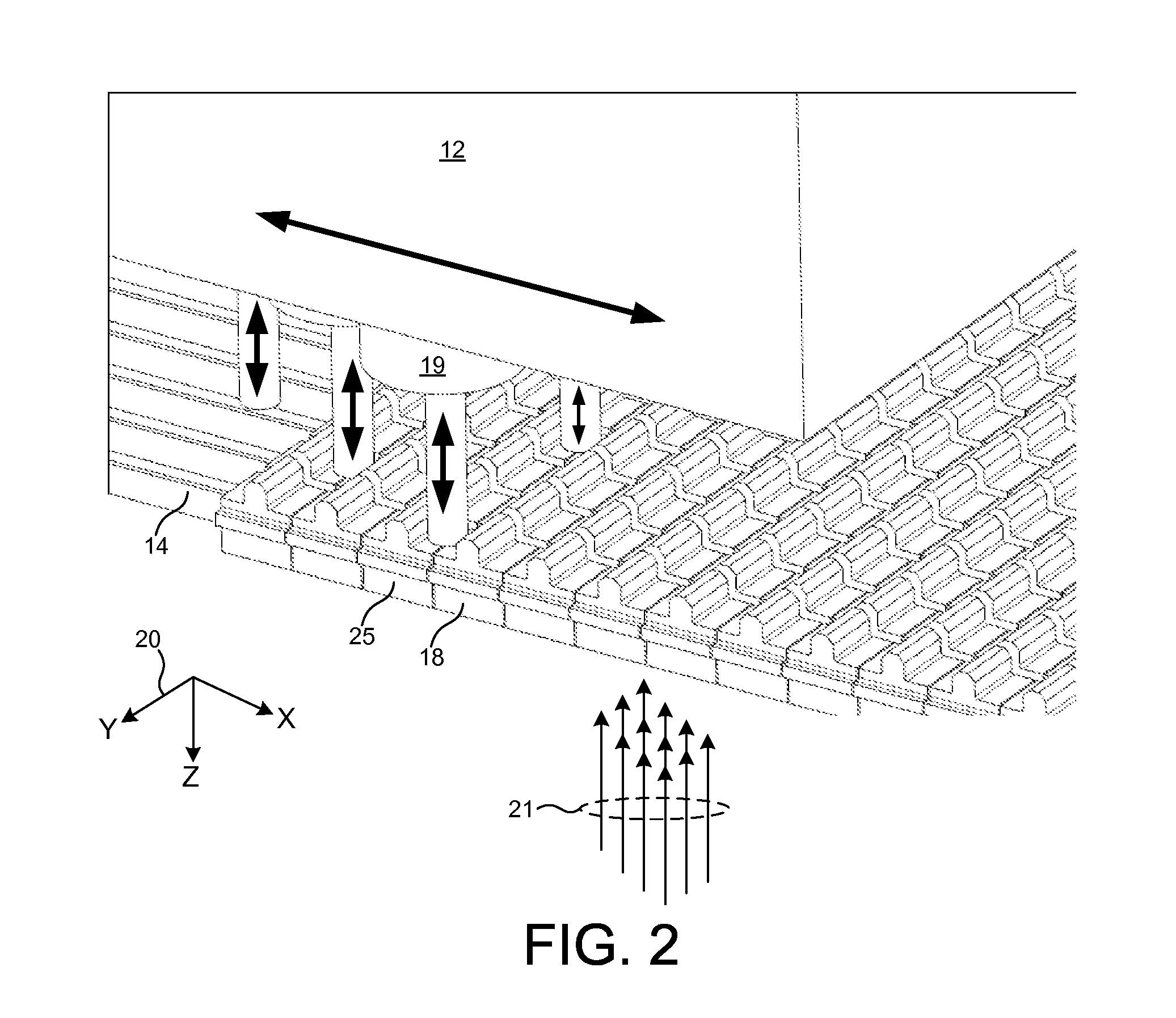
[0033]An aperture mechanism programmable in two dimensions is introduced to increase the range of measurement applications accommodated by the measurement system with increased sensitivity, while maintaining adequate throughput necessary for modern semiconductor manufacture.

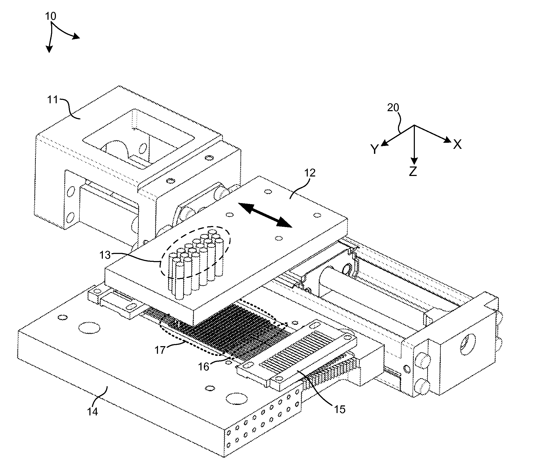
[0034]FIG. 1 illustrates a programmable aperture system 10 in one embodiment. The programmable aperture system 10 includes a two dimensional array of mechanical pixels 17 that selectively block light passing through the aper...


PUM

PropertyMeasurementUnit
diameteraaaaaaaaaa
wavelength rangeaaaaaaaaaa

Abstract

Methods and systems for reconfiguring an aperture of an optical inspection system are presented. A programmable aperture system includes a two dimensional array of mechanical pixels that selectively block light passing through the aperture. An array of linear guiding elements is aligned parallel to one another, and each row of mechanical pixels is supported by a corresponding linear guiding element. Each mechanical pixel is configured to slide along the corresponding linear guiding element when pushed by an actuator subsystem. The actuator subsystem repositions one or more of the mechanical pixel elements to change the shape of the aperture. The actuator subsystem is configured to selectively engage one or more mechanical pixel elements and translate the one or more mechanical pixel elements along corresponding linear guiding elements to a new position.

Description

CROSS REFERENCE TO RELATED APPLICATION[0001]The present application for patent claims priority under 35 U.S.C. §119 from U.S. provisional patent application Ser. No. 61 / 837,034, entitled “2D Programmable Aperture Mechanism,” filed Jun. 19, 2013, the subject matter of which is incorporated herein by reference in its entirety.TECHNICAL FIELD[0002]The described embodiments relate to optical inspection systems and methods, and more particularly to methods and systems for improved aperture mechanisms for shaping light within an optical inspection system.BACKGROUND INFORMATION[0003]Semiconductor devices such as logic and memory devices are typically fabricated by a sequence of processing steps applied to a specimen. The various features and multiple structural levels of the semiconductor devices are formed by these processing steps. For example, lithography among others is one semiconductor fabrication process that involves generating a pattern on a semiconductor wafer. Additional example...

Claims


Application Information

Patent Timeline
Patent Type & Authority Patents(United States)
IPC IPC(8): G01N21/00G01N21/88G01N21/95G02B26/02
CPCG01N21/8806G01N21/9501G02B26/02
Inventor BRUNNER, RUDOLF
Owner KLA CORP
Why Eureka
Try Eureka