Surface-emission laser diode operable in the wavelength band of 1.1-1.7 micrometers and optical telecommunication system using such a laser diode

a laser diode and surface-emission technology, applied in the field of laser diodes, can solve the problems of reducing the resistance of the laser diode, difficult to use the surface-emission laser diode with the integrated circuit of the driver, and the comparatively high operating voltage of the 2.5 volt or more operating voltage, so as to reduce the area of the n-type semiconductor, reduce the electrostatic capacitance of the heterointerface, and reduce the effect of the area

Inactive Publication Date: 2009-09-15
RICOH KK
View PDF46 Cites 9 Cited by
  • Summary
  • Abstract
  • Description
  • Claims
  • Application Information

AI Technical Summary

Benefits of technology

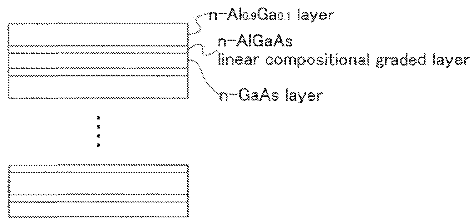
[0133]In another aspect, there is provided a surface-emission laser diode of the type as set forth above, wherein said n-type semiconductor distributed Bragg reflector comprises stacking of first and second semiconductor layers having respective refractive indices different from each other, said n-type semiconductor distributed Bragg reflector further including an intermediate layer having a refractive index intermediate of said refractive indices of said first and second semiconductor layers between said first and second semiconductor layers with a thick larger than 20 [nm]. By using the construction of the foregoing embodiment, it becomes possible to reduce the area of the n-type semiconductor distributed Bragg reflector contributing to the electrostatic capacitance by confining the path of the electrons current, and the electrostatic capacitance of the heterointerface of the n-type semiconductor distributed Bragg reflector is reduced. Thereby, high speed modulation becomes possible. Thus, as explained in relation to the effect of the invention before, the potential distribution as the heterointerface is smoothed by providing the foregoing semiconductor layer to the heterointerface as compared with the case in which such an intermediate layer is not provided, and depletion or accumulation of carriers is suppressed. Thereby, the electrostatic capacitance caused by the depletion or accumulation of the carriers can be reduced drastically. Further, by restricting the path of the electrons in the mesa region by etching and increasing of resistance of the n-type distributed Bragg reflector as in the case of some embodiments, the area of the distributed Bragg reflector contributing to the capacitance is reduced. Thus, by combining these features as in the case of some embodiment, the electrostatic capacitance of the device is reduced more effectively, and a structure very well suited for high speed modulation is obtained. The device of such an embodiment can perform high speed modulation of 10 Gbps or more as a result of decrease of the electrostatic capacitance of the n-type distributed Bragg reflector.
[0134]According to another aspect, there is provided a surface-emission laser diode of the type as set forth above, wherein said n-type semiconductor distributed Bragg reflector comprises stacking of a first and second semiconductor layers having respective refractive indices different from each other, said n-type semiconductor distributed Bragg reflector further including an intermediate layer having a refractive index intermediate of said first and second semiconductor layers between said first and second semiconductor layers with a thickness of 30 [nm] or more. By using the construction of the tenth embodiment, it becomes possible to reduce the area of the n-type semiconductor distributed Bragg reflector contributing to the electrostatic capacitance by confining the path of the electron current, and it becomes possible to reduce the electrostatic capacitance of the heterointerface of the n-type semiconductor distributed Bragg reflector. Thereby, high speed modulation becomes possible. Thus, as explained in relation to the effect of the invention before, it becomes possible to smooth the potential distribution at the heterointerface sufficiently by providing the foregoing semiconductor layer to the heterointerface as compared with the case in which such an intermediate layer is not provided, and depletion or accumulation of carriers is suppressed. Thereby, the electrostatic capacitance caused by the depletion or accumulation of the carriers can be reduced more drastically. Further, by restricting the path of the electrons in the mesa region by etching and increasing of resistance of the n-type distributed Bragg reflector as in the case of some embodiments, the area of the distributed Bragg reflector contributing to the capacitance is reduced. Thus, by combining these features as in the case of some embodiment, the electrostatic capacitance of the device is reduced more effectively, and a structure very well suited for high speed modulation is obtained. The device of claim 10 can perform high speed modulation of 10 Gbps or more as a result of decrease of the electrostatic capacitance of the n-type distributed Bragg reflector.
[0135]According to another aspect, there is provided a surface-emission laser diode of the type as set forth before, wherein said n-type semiconductor distributed Bragg reflector comprises stacking of first and second semiconductor layers having respective refractive indices different from each other, said n-type semiconductor distributed Bragg reflector further including an intermediate layer having a refractive index intermediate of said first and second semiconductor layers, between said first and second semiconductor layers with a thickness t [nm] determined with respect to a reflection wavelength λ [um] of said distributed Bragg reflector so as to fall in the ranges of 20<t≦(50 λ−15) [nm].
[0136]By using the construction of the eleventh embodiment, it becomes possible to reduce the area of the n-type semiconductor distributed Bragg reflector contributing to the electrostatic capacitance by confining the path of the electrons current, and the electrostatic capacitance of the heterointerface of the n-type semiconductor distributed Bragg reflector is reduced. Thereby, high speed modulation becomes possible. Thus, as explained in relation to the effect of the invention, the potential distribution as the heterointerface is smoothed by providing the foregoing semiconductor layer to the heterointerface as compared with the case in which such an intermediate layer is not provided, and depletion or accumulation of carriers is suppressed. Thereby, the electrostatic capacitance caused by the depletion or accumulation of the carriers can be reduced drastically. Further, by choosing the thickness of the intermediate layer to the foregoing range, it becomes possible to maintain the reflectivity of the n-type distributed Bragg reflector, and a surface-emission laser diode of low oscillation threshold is obtained.
[0137]Further, by restricting the path of the electrons in the mesa region by etching and increasing of resistance of the n-type distributed Bragg reflector as in the case of some embodiments, the area of the distributed Bragg reflector contributing to the capacitance is reduced. Thus, by combining these features as in the case of some embodiment, the electrostatic capacitance of the device is reduced more effectively, and a structure very well suited for high speed modulation is obtained. The device of claim 11 can perform high speed modulation of 10 Gbps or more as a result of decrease of the electrostatic capacitance of the n-type distributed Bragg reflector.
[0138]According to the invention, the active layer may be formed of a group III element and a group V element, said group III element of said active layer being any or all of Ga and In, said group V element of said active layer being any or all of As, N, Sb and P in the surface-emission laser diode. Thus, the electrostatic capacitance is reduced and it becomes possible to provide a surface-emission laser diode of long wavelength band and capable of performing high speed modulation.

Problems solved by technology

Thereby, there arises a problem in that the semiconductor multilayer part increases the resistance of the laser diode.
Because of this, conventional surface-emission laser diodes constructed on a GaAs substrate have suffered from the problem of comparatively high operating voltage of about 2.5 volts or more.
Because of this, it has been difficult to use the surface-emission laser diode with a CMOS driver integrated circuit, which produces a laser driving voltage of 2 volts at best.
In order to reduce the operational voltage below 2 V, it is necessary to reduce the device resistance by one-half, while it is extremely difficult to meet for this requirement at the present stage of technology.
Unfortunately, the desired low voltage operation is not materialized in such a long wavelength laser diode.
In such a system, the lattice constant of InP constituting the substrate is large, and it is difficult to achieve a large refractive-index difference in the reflector when a material that achieves lattice matching with the InP substrate is used for the reflector.
In such a construction, however, the resistance of the reflector increases again as a result of increased stacking number of the reflector.
Thus, it has been difficult to drive the laser diode driver by a CMOS integrated circuit.
In a surface-emission laser diode formed on an InP substrate, there is another problem of change of laser characteristic caused by the temperature.
However, the use of such a temperature regulator is difficult in the apparatus for home use, which is subjected to a severe demand of cost reduction.
Because of these problems of increased number of stacking in the reflector and the poor temperature characteristics, practical long-wavelength surface-emission laser diode has not yet commercialized.
However, the laser diode structure thus formed does not provide optical emission at all, or operates but only with low power, indicating that the efficiency of optical emission is extremely small.
In this case, too, the luminous efficacy of the laser diode is far from the level of practical use.
More specifically, it is thought that the use of a material containing Al easily invites formation of crystal defects originating from Al.
Thus, the stacking number in the reflector has to be increased, and the object of reducing the resistance of the surface-emission laser diode is not attained.
Thus, at present, the surface-emission laser diode operable at the long-wavelength of 1.1-1.7 μm does not exist, and because of this, it is not possible to construct a computer network or optical-fiber telecommunication system that uses such a laser diode.
As explained before, in a conventional surface-emission laser diode, it was also not possible to use a CMOS circuit for the laser diode driver, and it has been necessary to use an expensive special driver circuit.
Unfortunately, the surface-emission laser diode that can be used for this purpose and can be used with a low-cost CMOS driver integrated circuit, and oscillates at the long-wavelength band of 1.1-1.7 μm does not exist.
Meanwhile, in the abovementioned semiconductor Bragg reflector, in which semiconductor layers of different bandgaps are grown alternately, there arises the problem of spike formation in the band structure thereof at the hetero interface as a result of the band discontinuity.
Thus, there arises a problem in that the electric resistance becomes very high in the semiconductor multilayer part of the surface-emission laser diode.
As noted previously, it has been difficult to drive a laser diode having such a large driving voltage by the driver integrated circuit formed of a CMOS circuit (driving voltage is below 2 volts).
However, this is a very difficult subject.
However, the surface-emission laser diode that can be used for this purpose and can be used with a low-cost CMOS driver integrated circuit, and oscillates at the long-wavelength band of 1.1-1.7 μm does not exist yet.
However, the photodetection device that has sensitivity to the desired wavelength band of 1.1-1.7 μm is expensive as compared with the low cost Si photodetection device.
Thus, simple replacement of a conventional Si photodetection device with the photodetection device having the sensitivity to the wavelength of 1.1-1.7 μm causes an increase of cost of the whole optical-fiber telecommunication system.
In such a laser diode, deterioration of device characteristic may be caused as a result of the thermal stress caused by the difference of linear thermal expansion coefficient with regard to the mounting substrate.
This issue is related to the yield of the laser diode production process.
Summarizing above, there is no available long-wavelength surface-emission laser diode operable at the wavelength band of 1.1-1.7 μm and that there is no available optical transmission / reception system that uses such a laser diode.
In the device in which the confinement diameter is reduced to about 4 μm or less as noted above, on the other hand, there arises a problem of increased electrical resistance because of excessive decrease of the current path area in the current confinement structure.
As such increase of resistance of the device can become the cause of various problems such as increase of operational voltage, saturation of output power caused by heating, decrease of modulation speed, and the like, it is necessary to reduce the resistance of the confinement structure.
In the case of using a highly doped p-type semiconductor, it is true that the electric characteristics such as device resistance are improved, while there also arise problems such as conspicuous free carrier absorption caused by holes or conspicuous intra-valence band absorption.
However, such a construction, while being able to reduce the resistance to some extent by reducing the bandgap difference for the semiconductor layers constituting the heterointerface, has still suffered from the problem that the electric resistance cannot be reduced sufficiently due to the fact that the reduction of doping concentration inevitably increases the adversary effect of the heterointerface.
Further, the device of Japanese Laid-Open Patent Application 2001-332812 suffers from the problem in that the reduction of bandgap difference leads to decrease of reflectivity of the semiconductor distributed Bragg reflector and penetration of light into the semiconductor distributed Bragg reflector is increased.
Particularly, a depletion layer characterized by decreased carrier density forms electrostatic capacitance component, and become of this, restriction is imposed to electric characteristics and device response characteristics when a device (surface-emission laser diode, and the like) is driven to cause pulse operation or high speed modulation.
Furthermore, because of the influence of the heterointerface, there is caused the problem in that non-linearity is caused in the current-voltage characteristic and that the current-voltage characteristic changes in response to the difference of the drive condition of the device.

Method used


Image

  • Surface-emission laser diode operable in the wavelength band of 1.1-1.7 micrometers and optical telecommunication system using such a laser diode
  • Surface-emission laser diode operable in the wavelength band of 1.1-1.7 micrometers and optical telecommunication system using such a laser diode
  • Surface-emission laser diode operable in the wavelength band of 1.1-1.7 micrometers and optical telecommunication system using such a laser diode

Examples


tenth embodiment

[0680]FIG. 63 shows the example of a telecommunication system that uses the long-wavelength surface-emission laser diode chip 32 with the laser oscillation wavelength 1.1-1.7 μm band with plural optical fibers. Those parts explained previously in the FIG. 63 are designated with the same reference numerals and explanation is omitted.

[0681]In the construction of FIG. 63, the laser diode 32A in the laser diode chip 32 is driven by a communication control unit 81 via a laser diode driver circuit 82. The optical signal is supplied to the optical fibers 72 and 73 in the form of an optical beam.

[0682]Conventionally, an optical telecommunication system was studied by using the laser oscillation wavelength of 0.85 μm. However, because of the large transmission loss in the optical fiber, it was not practical for long distance telecommunication. Further, in the case of the telecommunication system that uses the plural optical fibers in combination of conventional edge-emission type laser diode...

eleventh embodiment

[0693]FIG. 69 shows an example of the optical fiber 101 used in a telecommunication system that uses a long-wavelength surface-emission laser diode. Those parts explained previously are designated by the same reference numerals and the description thereof will be omitted.

[0694]FIG. 69 is referred to. The optical fiber 101 is injected with the laser beam emitted from the laser diode emission part 32A. The optical fiber 101 consists of cladding 101B enclosing a core 101A, and the core 101 A transmits the laser beam thus injected. The diameter D of the core 101A is determined with regard to the length L so as to satisfy the condition 105≦L / D≦109.

[0695]Conventionally, an optical telecommunication system was studied by using the laser oscillation wavelength of the 0.85 μm band. However, the transmission loss of the optical fiber was too large and there was no practical value. Also there was no laser diode that can oscillate stably in the long-wavelength band, in which the transmission lo...

twelfth embodiment

[0718]FIGS. 74A and 74B show an example of a laser diode chip 120 that is used with the optical telecommunication system in which the long-wavelength surface-emission laser diode of the present invention is used, wherein FIG. 74A shows a plane view while FIG. 74B shows a cross-sectional view taken along a line A-A′. It should be noted that the scale FIG. 74A is not identical with the scale of FIG. 74B. In the drawings, those parts explained previously are designated by the same reference numerals and the description thereof will be omitted.

[0719]FIGS. 74A and 74B are referred to.

[0720]It can be seen that the long-wavelength surface-emission laser diode 32A and the photodetection device 34A are formed to monolithically on a laser diode chip 120.

[0721]The photodetection device 34A has a stacked structure similar to the stacked structure of the long-wavelength surface-emission laser diode 32A and is formed simultaneously with the process of forming the surface-emission laser diode 32A....


PUM


Abstract

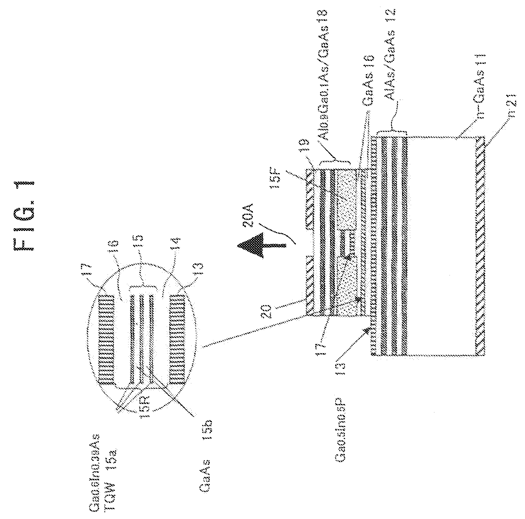
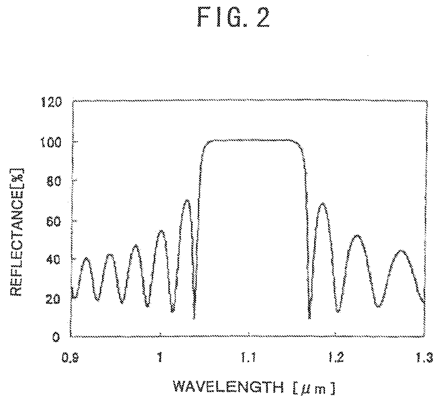
A surface-emission laser diode includes a distributed Bragg reflector tuned to wavelength of 1.1 μm or longer, wherein the distributed Bragg reflector includes an alternate repetition of a low-refractive index layer and a high-refractive index layer, with a heterospike buffer layer having an intermediate refractive index interposed therebetween with a thickness in the range of 5-50 nm.

Description

CROSS REFERENCE TO RELATED APPLICATIONS[0001]This application is a divisional of U.S. application Ser. No. 10 / 697,035 filed on Oct. 31, 2003, which is a continuation-in-part of U.S. application Ser. No. 10 / 085,204 filed on Feb. 26, 2002, all of which claim priority to Japanese Patent Application No. 2001-050083 filed on Feb. 26, 2001, Japanese Patent Application No. 2001-050145 filed on Feb. 26, 2001, Japanese Patent Application No. 2001-050171 filed on Feb. 26, 2001, Japanese Patent Application No. 2001-051253 filed on Feb. 26, 2001, Japanese Patent Application No. 2001-051256 filed on Feb. 26, 2001, Japanese Patent Application No. 2001-051266 filed on Feb. 26, 2001, Japanese Patent Application No. 2001-053190 filed on Feb. 27, 2001, Japanese Patent Application No. 2001-053200 filed on Feb. 27, 2001, Japanese Patent Application No. 2001-053213 filed on Feb. 27, 2001, Japanese Patent Application No. 2001-053218 filed on Feb. 27, 2001, Japanese Patent Application No. 2001-053225 file...

Claims


Application Information

Patent Timeline
Patent Type & Authority Patents(United States)
IPC IPC(8): H01S5/00
CPCB82Y20/00G02B5/285G02B6/4202G02B6/4246G02B6/43H01S5/18308G02B5/0833H01L2224/48091G02B6/4214H01S5/0014H01S5/005H01S5/02248H01S5/02284H01S5/02296H01S5/0262H01S5/0264H01S5/0683H01S5/18311H01S5/18358H01S5/3215H01S5/34306H01S5/423H01S2301/173H01L2924/00014H01L2924/12044H01S5/02251H01S5/02257H01S5/02325H01L2924/00
Inventor JIKUTANI, NAOTOSATO, SHUNICHITAKAHASHI, TAKASHIITOH, AKIHIROSEKIYA, TAKUROSAKURAI, AKIRAKATOH, MASAYOSHIFURUTA, TERUYUKIMIYAGAKI, KAZUYAKANAI, KENWATADA, ATSUYUKISUZUKI, KOEISUGAWARA, SATORUSATOH, SHINJIHIKICHI, SHUUICHI
Owner RICOH KK
Why Eureka
Try Eureka