Semiconductor light-emitting device having double encapsulating structure
a semiconductor and light-emitting technology, applied in the direction of semiconductor devices, semiconductor/solid-state device details, radiation control devices, etc., to achieve the effect of excellent optical characteristics and simple structur
- Summary
- Abstract
- Description
- Claims
- Application Information
AI Technical Summary
Benefits of technology
Problems solved by technology
Method used
Image


Examples
first embodiment
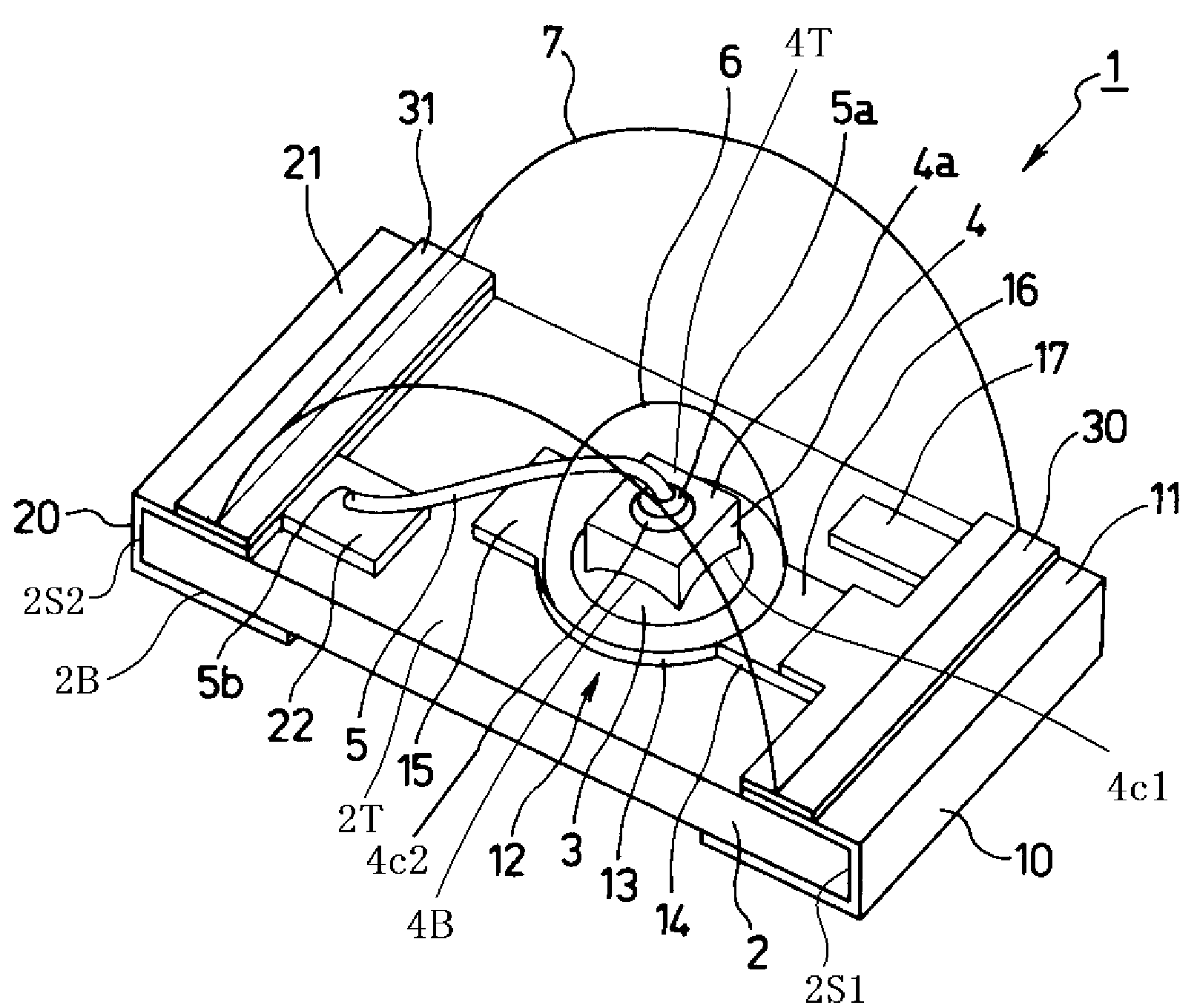
[0046]The above-described elements will now be described with reference to FIGS. 2a and 2b, which are enlarged top views showing the semiconductor light-emitting device, wherein FIG. 2b abbreviates some marks to show an exemplary wavelength converting material contained in the first encapsulating material 6 and to show exemplary major dimensions. As the circuit board 2, a resin board such as a silicone resin board, a glass epoxy board and the like, a metallic board such as an aluminum substrate, an iron substrate and the like, and a ceramic substrate can be used.
[0047]The die-bonding portion 12 of the first conductor pattern 10 can include: the die-bonding pad 13 formed in a substantially circular shape, and being located in the middle portion on the top surface 2T of the circuit board 2; the connecting portion 14 electrically connecting between the die-bonding pad 13 and the first external electrode 11 of the first conductor pattern 10; the die-bonding projection pattern 15 extendi...
second embodiment
[0074]Next, evaluating results with respect to the first encapsulating material 6 of the semiconductor light-emitting device 1A will now be described. In the semiconductor light-emitting device 1A of the second embodiment, a diameter D of the die-bonding pad 13 formed in a substantially circular shape of the first conductor pattern 10 is 0.54 millimeters, and each of the first length L1 of the die-bonding projection pattern 15 and the second length L2 of the exposed connecting portion 16 is 0.2 millimeters as shown in FIG. 2b.
[0075]In the semiconductor light-emitting device 1A of the second embodiment, a semiconductor light-emitting chip having a top surface 4T, which is formed in a rectangular shape having opposite sides of 0.22 millimeters and other opposite sides of 0.27 millimeters, is employed as the semiconductor light-emitting chip 4. The semiconductor light-emitting chip 4 is die-bonded on the die-bonding pad 13 so that each of the side surfaces in the longitudinal directio...
PUM
 Abstract
Description
Claims
Application Information
 - R&D
- Intellectual Property
- Life Sciences
- Materials
- Tech Scout
- Unparalleled Data Quality
- Higher Quality Content
- 60% Fewer Hallucinations
Browse by: Latest US Patents, China's latest patents, Technical Efficacy Thesaurus, Application Domain, Technology Topic, Popular Technical Reports.
© 2025 PatSnap. All rights reserved.Legal|Privacy policy|Modern Slavery Act Transparency Statement|Sitemap|About US| Contact US: help@patsnap.com