Printed circuit board and control device for a vehicle transmission comprising the printed circuit board

a technology of printed circuit board and control device, which is applied in the direction of printed circuit parts, electrical apparatus casings/cabinets/drawers, connectors and pcb, etc., can solve the problems of low unit cost and uncomplicated bonding technology, and achieve the effect of reducing the overall thermal resistance of the printed circuit board, facilitating further dissipation, and thick supply voltage areas

Active Publication Date: 2016-02-16
ZF FRIEDRICHSHAFEN AG
View PDF24 Cites 10 Cited by
  • Summary
  • Abstract
  • Description
  • Claims
  • Application Information

AI Technical Summary

Benefits of technology

[0007]Advantageously, through the majority of micro-through-holes, topological structures may be created that have a beneficial impact on the thermal behavior of the printed circuit board. The dissipation of heat at a printed circuit board may take place through conducting paths or conducting surfaces, as the case may be, and through-holes or vias, as the case may be, in particular through their copper tubes. By thermally coupling with one another at least one outer layer of the printed circuit board, and at least one inner layer of the printed circuit board adjacent to the outer layer, through the use of the majority of micro-through-holes, the overall thermal resistance of the printed circuit board is reduced. In addition to improving the overall thermal resistance, improved heat capacity or thermal dissipation arises. In particular, the thermal resistance between the outer two layers of the printed circuit board can be reduced. Thus, through the majority of micro-through-holes, heat may be removed very quickly and across large areas, for example from a circuit heated during operation on a surface of the printed circuit board, into an inner area of the printed circuit board. In the inner area of the printed circuit board, the heat may be, on the one hand, distributed, and, on the other hand, diverted through additional through-holes to an opposite side of the printed circuit board, which can act as a heat sink. On the surface of the printed circuit board acting as a heat sink, heat may be quickly led across large areas from the inside of the printed circuit board through the majority of micro-through-holes. Thus, embodiments of the present invention offer the advantage of improved heat dissipation for printed circuit boards. This improvement in thermal behavior does not require the use of elaborate technologies, such as ceramic printed circuit boards. Thus, the unit costs may be kept low, and uncomplicated bonding technology (for example) may be used. For EMC strategies (EMC=electromagnetic compatibility), in accordance with the embodiments of the present invention, there is plenty of room on the printed circuit board for an EMC-robust design.
[0023]In this connection, one execution is such that the descriptions concerning a preferred number and a preferred arrangement of micro-through-holes likewise apply to via pads or to a group consisting of at least one via pad and one micro-through-hole, as one via pad preferably surrounds at least one micro-through-hole as described above. At least one group of micro-through-holes may comprise a matrix of micro-through-holes, which features (for example) three, four, five or six rows and / or columns of micro-through-holes. Thereby, the matrix need not be square or rectangular. The matrix may also feature rows and / or columns that are arranged in an offset manner. In particular, the spacing of adjacent micro-through-holes within at least one group may be between 0.5 mm and 0.85 mm. With a view to a group consisting of via pads, a maximum diameter of a via pad of up to 0.3 mm with a maximum diameter of the micro-through-hole of up to 0.1 mm is preferred, whereas the preferred spacing of up to a maximum of 0.85 mm is located between the opposite outer edges of two adjacent via pads. The embodiments described above offer the advantage that a large number of micro-through-holes may be housed on a small space. This improves the thermal properties of the printed circuit board.

Problems solved by technology

Thus, the unit costs may be kept low, and uncomplicated bonding technology (for example) may be used.

Method used


Image

  • Printed circuit board and control device for a vehicle transmission comprising the printed circuit board
  • Printed circuit board and control device for a vehicle transmission comprising the printed circuit board
  • Printed circuit board and control device for a vehicle transmission comprising the printed circuit board

Examples


Embodiment Construction

[0031]Reference will now be made to embodiments of the invention, one or more examples of which are shown in the drawings. Each embodiment is provided by way of explanation of the invention, and not as a limitation of the invention. For example features illustrated or described as part of one embodiment can be combined with another embodiment to yield still another embodiment. It is intended that the present invention include these and other modifications and variations to the embodiments described herein.

[0032]In the following description of the preferred embodiments of the present invention, elements shown in the various figures and elements having similar effects use the same or similar reference signs, whereas a repeated description of these elements is omitted.

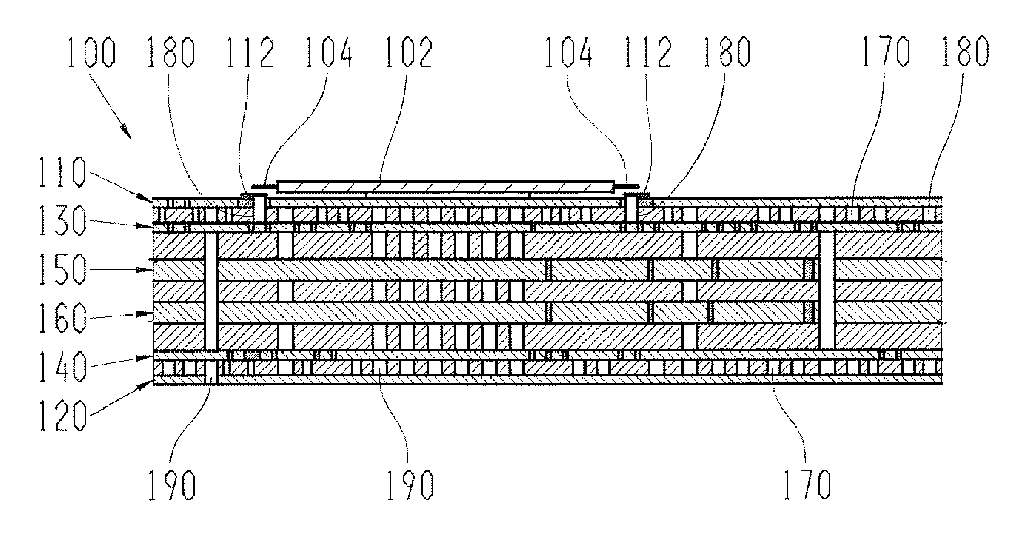
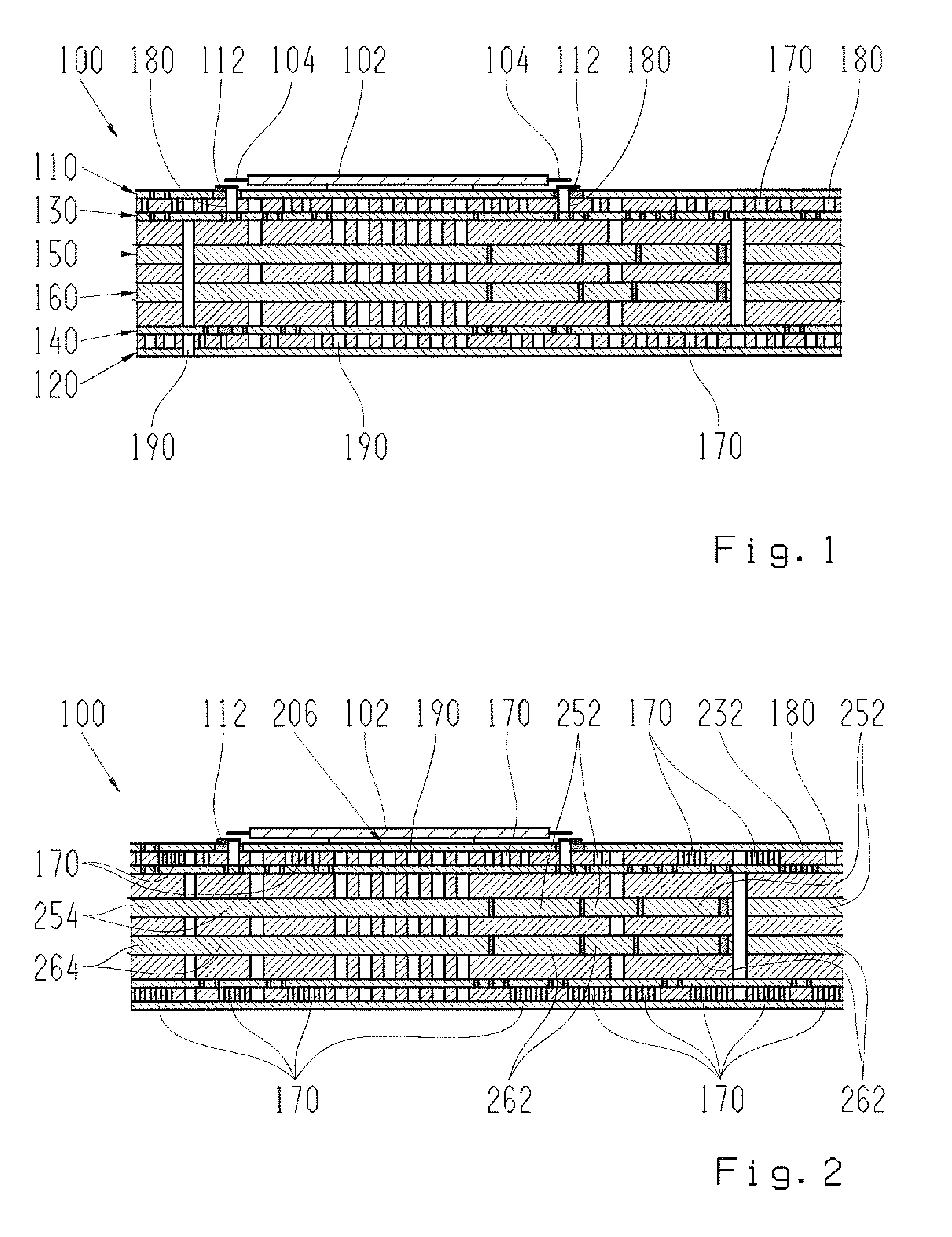
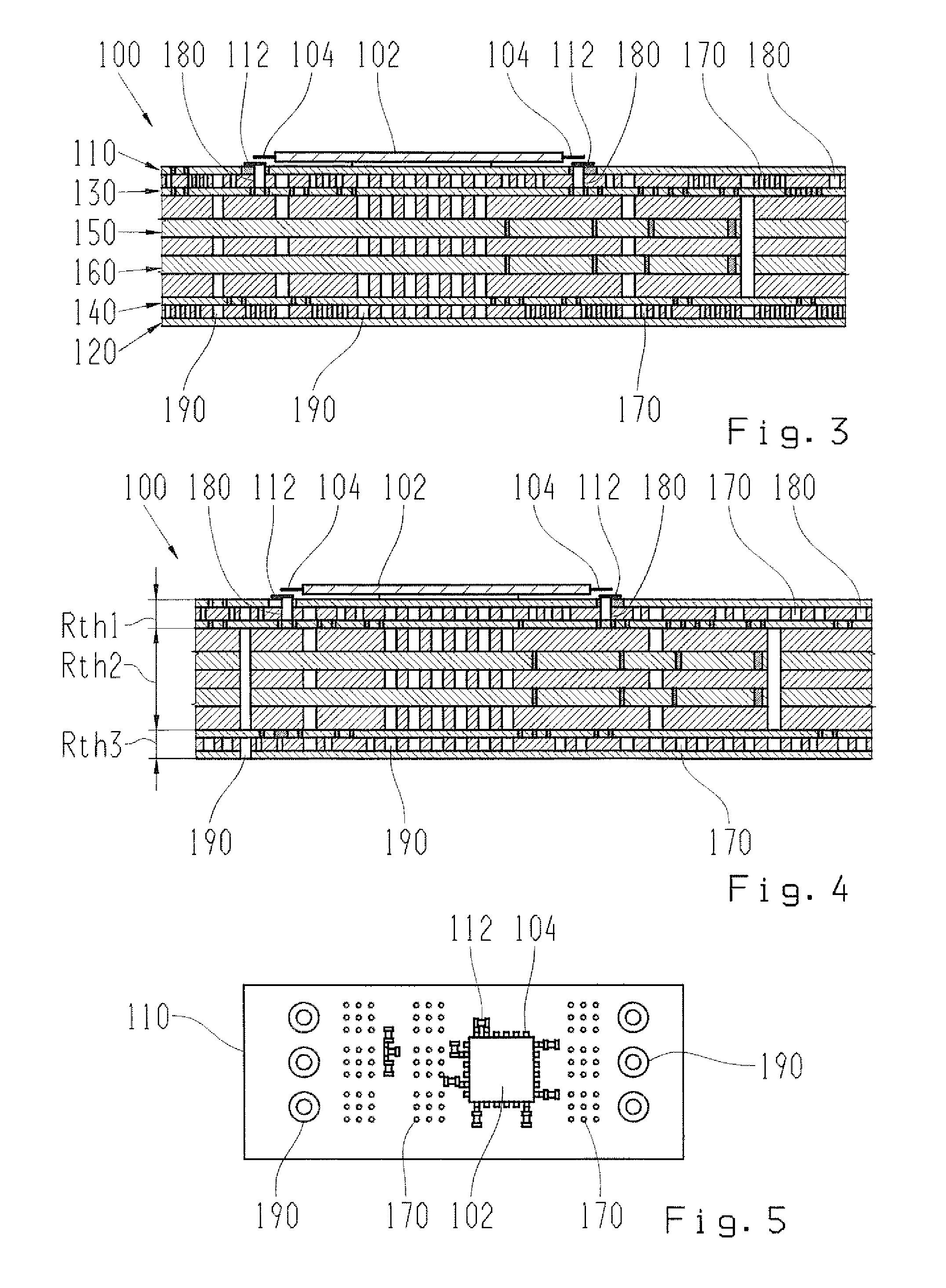
[0033]FIG. 1 shows a printed circuit board 100 in accordance with an embodiment of the present invention. Thereby, a section view of the printed circuit board 100 is shown in FIG. 1. The printed circuit board 100 is equip...


PUM


Abstract

The invention proposes a printed circuit board with multiple layers, which features at least one outer layer and at least one inner layer adjacent to the outer layer. The printed circuit board features a plurality of micro-through-holes, which are formed between a supply voltage area of at least one outer layer and a supply voltage area of at least one inner layer.

Description

FIELD OF THE INVENTION[0001]The present invention relates to a printed circuit board with multiple layers, and a control device for a transmission of a vehicle with the printed circuit board.BACKGROUND[0002]A multilayer printed circuit board, a so-called multilayer board, consists of multiple contact layers, such as ground and power layers. Furthermore, there are signal layers for unbundling the connections from the circuit diagram. The individual layers are isolated from one another and are filled with epoxy-reinforced glass fiber material, such as FR4 material. Conducting paths and technologies have the task of making connections, even through all layers. FR4, one of the materials that is primarily used, is a poor conductor of heat.[0003]DE 10 2008 029 410 A1discloses a device for conducting current. The device comprises an element that generates heat, a printed circuit board on which the element generating heat is applied, and a heat sink that is thermally coupled for dissipating...

Claims


Application Information

Patent Timeline
Patent Type & Authority Patents(United States)
IPC IPC(8): H05K1/00H05K5/00H05K1/02H05K1/11H05K3/46
CPCH05K1/115H05K1/0201H05K1/0206H05K1/0207H05K5/0082H05K3/4608H05K2201/09309H05K2201/09663H05K2201/09781
Inventor LASSMANN, WILFRIEDBUTTNER, CHRISTIAN
Owner ZF FRIEDRICHSHAFEN AG
Why Eureka
Try Eureka