Radiation detection apparatus and radiation detection system

a radiation detection apparatus and radiation detection technology, applied in the direction of x/gamma/cosmic radiation measurement, radioation controlled devices, instruments, etc., can solve the problems of increasing reducing the dynamic range of the radiation detection apparatus, and easily forming leakage paths on the side walls of the semiconductor layer. , to achieve the effect of reducing the residual charg

Active Publication Date: 2016-03-08
CANON KK
View PDF39 Cites 22 Cited by
  • Summary
  • Abstract
  • Description
  • Claims
  • Application Information

AI Technical Summary

Benefits of technology

[0005]In the radiation detection apparatus described in Japanese Patent Laid-Open No. 2013-012697, a residual charge readily occurs, which will be described later. An aspect of the present invention provides a technique for reducing the residual charge in a radiation detection apparatus having a conversion element in which the periphery of a semiconductor layer is positioned outside the periphery of an electrode.

Problems solved by technology

However, in the structure in which the semiconductor layer is separated into islands, a leakage path is readily formed on the side wall of the semiconductor layer.
The formation of the leakage path has adverse effects such as an increase in reverse dark current and a decrease in the dynamic range of the radiation detection apparatus.

Method used


Image

  • Radiation detection apparatus and radiation detection system
  • Radiation detection apparatus and radiation detection system
  • Radiation detection apparatus and radiation detection system

Examples


Embodiment Construction

[0021]Embodiments of the present invention will be described below with reference to the accompanying drawings. The same reference numerals denote the same components throughout various embodiments, and a repetitive description will be omitted. The embodiments can be appropriately changed and combined.

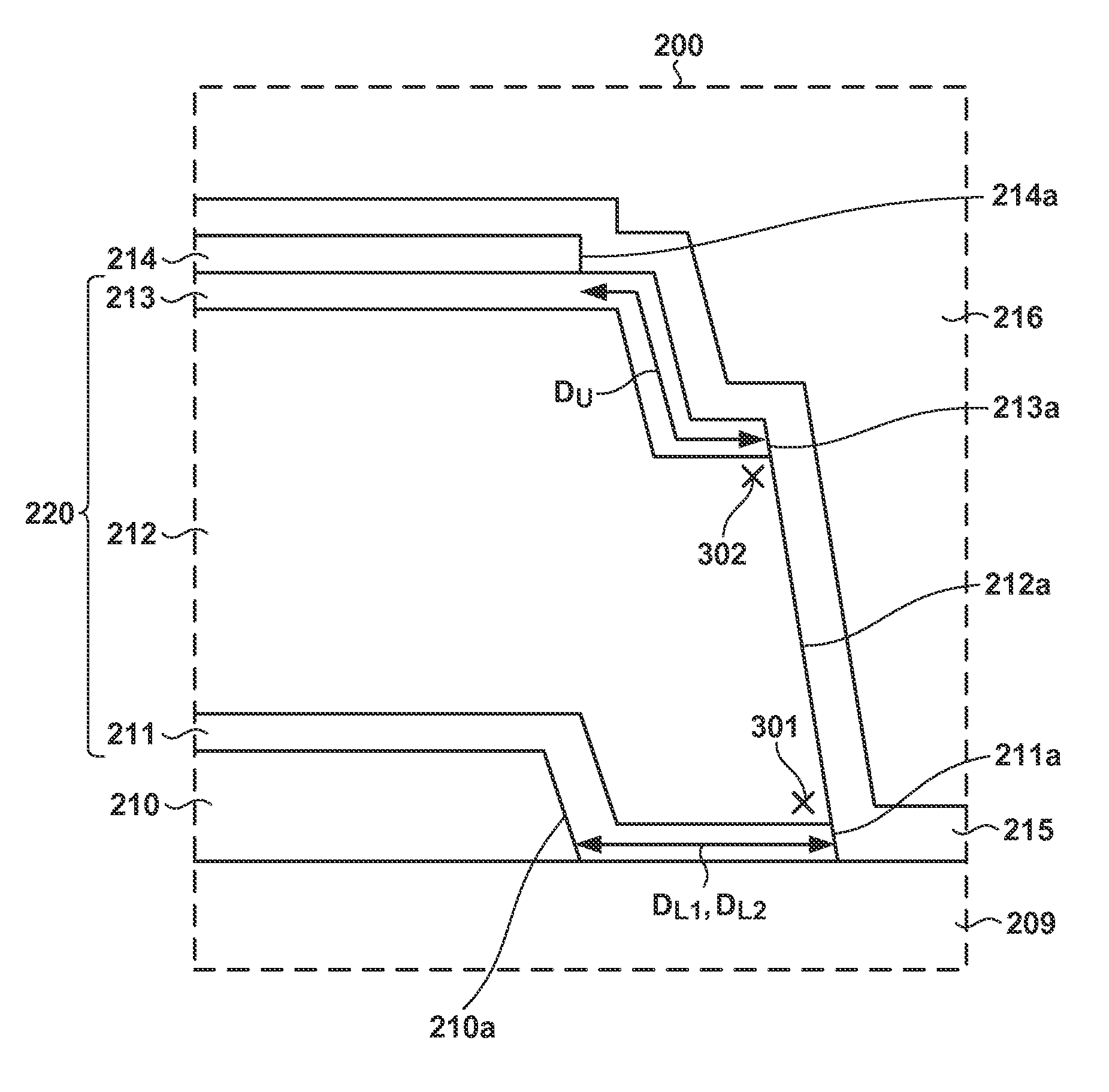
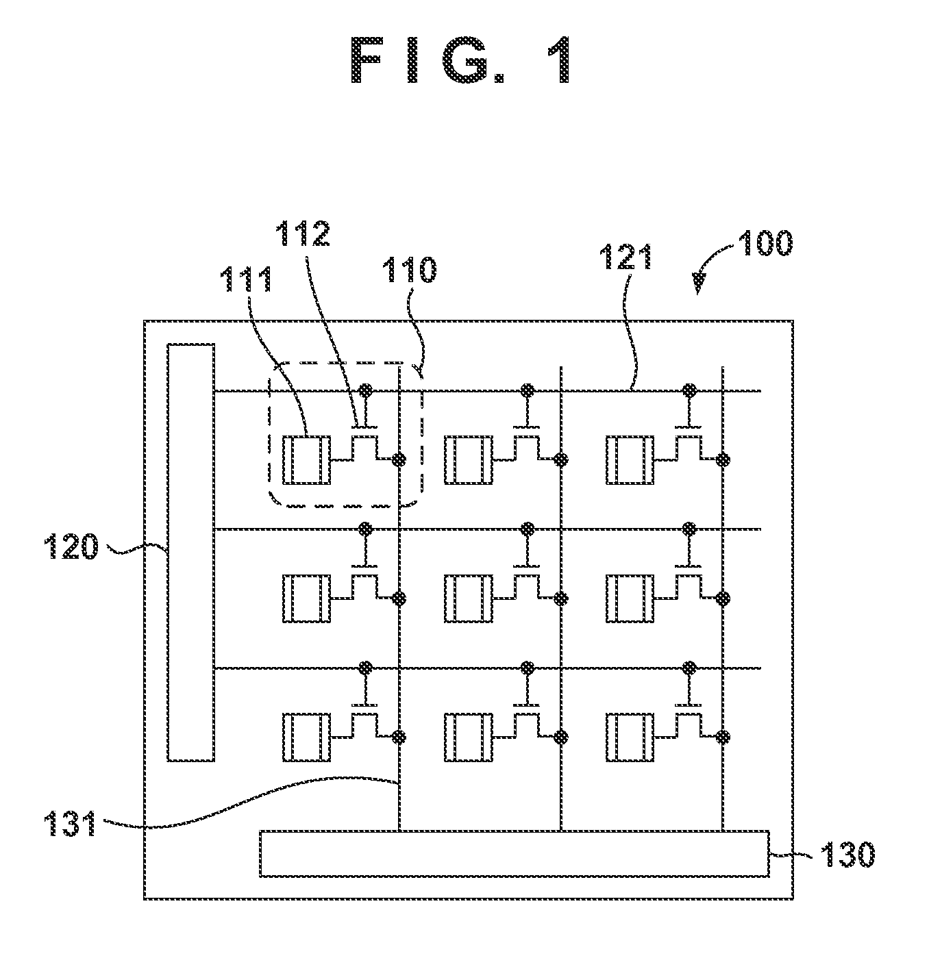
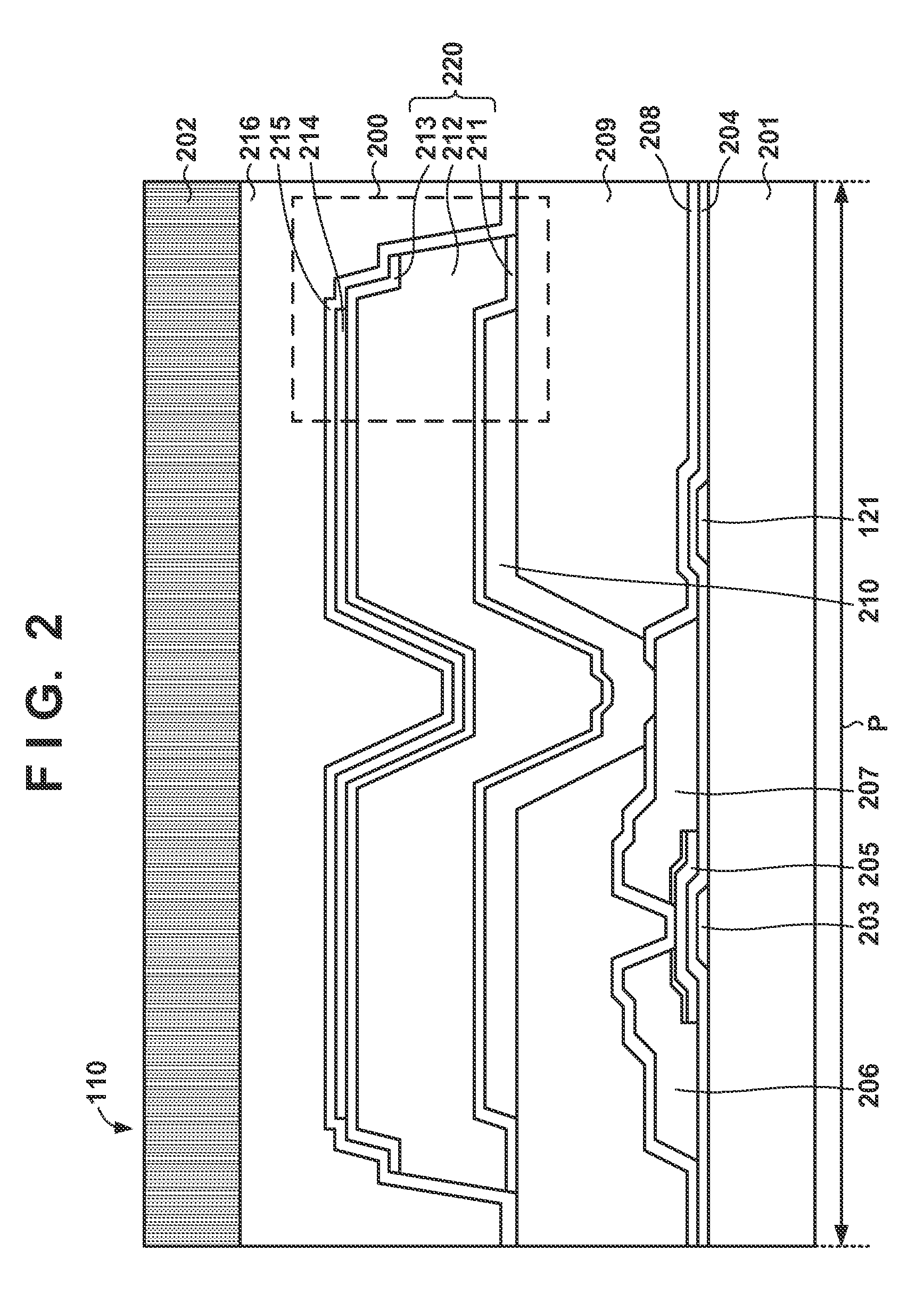
[0022]A radiation detection apparatus 100 according to some embodiments will be explained with reference to FIGS. 1 to 5. The radiation detection apparatus 100 is used for, for example, a medical image diagnostic apparatus, a nondestructive inspection apparatus, an analysis apparatus using radiation, or the like. FIG. 1 is a schematic equivalent circuit diagram of the radiation detection apparatus 100. The radiation detection apparatus 100 includes a plurality of pixels 110. The plurality of pixels 110 are arranged in a two-dimensional matrix to constitute a pixel array. Each pixel 110 includes a conversion element 111 and a switching element 112. The conversion element 111 is connecte...


PUM


Abstract

A radiation detection apparatus includes conversion elements including a first electrode, a semiconductor layer, and a second electrode that are divided for each pixel; switching elements electrically connected to the first electrodes; and a first insulating layer that separates the conversion elements of adjacent pixels. The semiconductor layer is located between the first and second electrodes. A periphery of the semiconductor layer is located outside peripheries of the first and second electrodes. The semiconductor layer includes a first impurity semiconductor layer, a second impurity semiconductor layer, and an intrinsic semiconductor layer located between the first and second impurity semiconductor layers. Parameters of the apparatus are defined to set a residual charge 10 μs after the switching element is turned on to be not higher than 2%.

Description

BACKGROUND OF THE INVENTION[0001]1. Field of the Invention[0002]The present invention relates to a radiation detection apparatus and a radiation detection system.[0003]2. Description of the Related Art[0004]A radiation detection apparatus has been used, in which a plurality of pixels each having a combination of a conversion element and switching element are arranged. As the conversion element, a PIN diode or a MIS diode is used. In particular, a PIN structure in which a semiconductor layer is sandwiched between two electrodes can be easily manufactured, has a simple operation mechanism, and thus is widely used. By separating a semiconductor layer into islands for respective pixels, a sharp image with less crosstalk between pixels is obtained. However, in the structure in which the semiconductor layer is separated into islands, a leakage path is readily formed on the side wall of the semiconductor layer. The formation of the leakage path has adverse effects such as an increase in re...

Claims


Application Information

Patent Timeline
Patent Type & Authority Patents(United States)
IPC IPC(8): G01T1/20H01L27/146G01T1/29G01T1/24A61B6/00
CPCA61B6/4233G01T1/2018G01T1/2928H01L27/14663A61B6/50G01T1/20183
Inventor OFUJI, MASATOWATANABE, MINORUYOKOYAMA, KEIGOKAWANABE, JUNFUJIYOSHI, KENTAROWAYAMA, HIROSHI
Owner CANON KK
Why Eureka
Try Eureka