Photoelectric conversion devices and organic sensors and electronic devices

一种光电转换、有机光电转换的技术,应用在电固体器件、光伏发电、电气元件等方向,能够解决难以精确地预测有机材料特性、无法容易地控制光电转换器件所需性质等问题,达到提高电荷提取效率、提高电荷迁移率、减少残留电荷的效果

Pending Publication Date: 2020-11-17
SAMSUNG ELECTRONICS CO LTD
View PDF1 Cites 0 Cited by
  • Summary
  • Abstract
  • Description
  • Claims
  • Application Information

AI Technical Summary

Problems solved by technology

[0005] However, since such organic materials exhibit properties different from those of silicon due to high binding energy and exhibit recombination behavior associated with such organic materials, it is difficult to precisely predict the properties of organic materials and thus cannot be easily Controlling desired properties of photoelectric conversion devices

Method used


Image

  • Photoelectric conversion devices and organic sensors and electronic devices
  • Photoelectric conversion devices and organic sensors and electronic devices
  • Photoelectric conversion devices and organic sensors and electronic devices

Examples


example 1

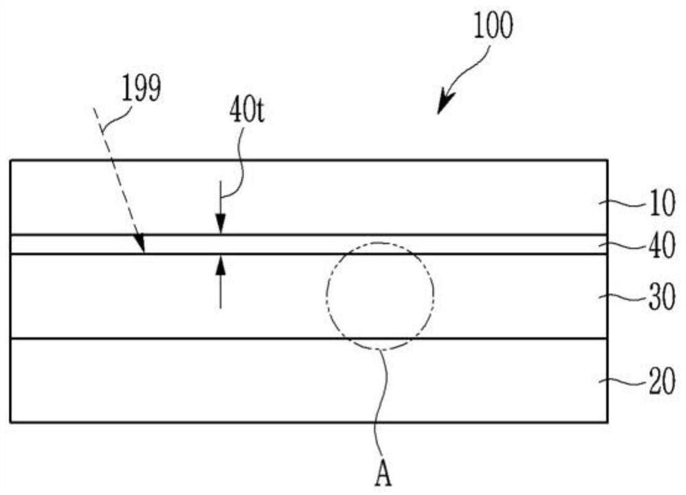
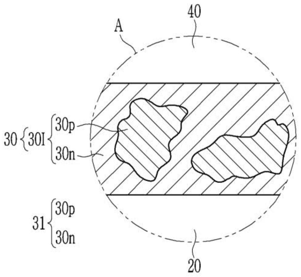
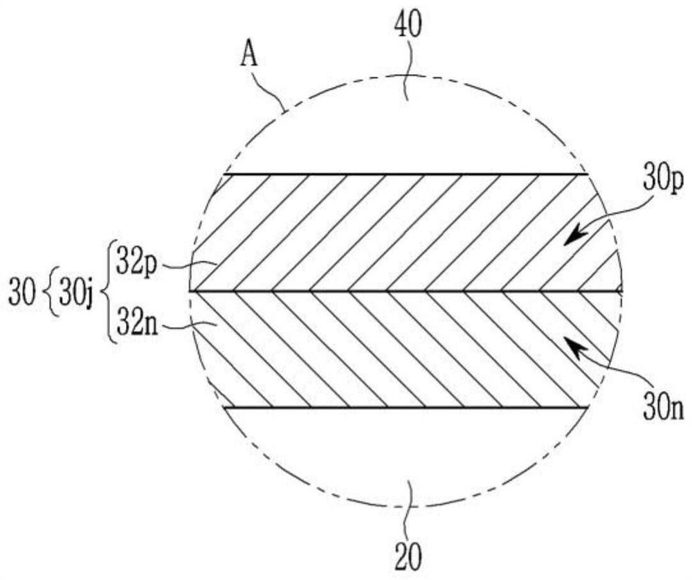
[0267] ITO was sputtered on a glass substrate to provide a 150 nm thick anode. Subsequently, the compound represented by Chemical Formula A was deposited on the anode to provide a 5 nm-thick charge blocking layer. Then, the p-type semiconductor (λ max : 545 nm) and an n-type semiconductor that is fullerene (C60) were co-deposited on the charge blocking layer at a volume ratio of 1.25:1 to provide a 100 nm thick photoelectric conversion layer. Yb (work function: 2.6eV) and GeO 2 was thermally evaporated on the photoelectric conversion layer at a weight ratio of 1:2 to provide a 2 nm thick charge assist layer. ITO (work function: 4.7 eV) was sputtered on the charge assist layer to provide a 7 nm thick cathode. Then, aluminum oxide (Al 2 o 3 ) was deposited on the cathode to provide a 40 nm thick anti-reflection layer and encapsulated with glass to provide a photoelectric conversion device.

[0268] [chemical formula A]

[0269]

[0270] [Chemical formula B-1]

[0271]...

example 2

[0273] Except for Yb and GeO 2 A photoelectric conversion device was fabricated according to the same procedure as in Example 1, except that it was thermally evaporated at a weight ratio of 1:3 to form a charge assisting layer.

example 3

[0275] ITO was sputtered on a glass substrate to provide a 150 nm thick anode. Subsequently, the compound represented by Chemical Formula A was deposited on the anode to provide a 5 nm-thick charge blocking layer. Then, a p-type semiconductor represented by Chemical Formula B-1 and an n-type semiconductor that is fullerene (C60) were co-deposited on the charge blocking layer at a volume ratio of 1.25:1 to provide a 100 nm-thick photoelectric conversion layer. Then, on the photoelectric conversion layer, Yb was thermally evaporated to form a 2nm-thick first charge auxiliary layer and GeO 2 was thermally evaporated to form a 0.5 nm-thick second charge assisting layer, thereby forming a two-layer charge assisting layer. ITO was sputtered on the two-layer charge assist layer to provide a 7 nm thick cathode. Then, aluminum oxide (Al 2 o 3 ) was deposited on the cathode to provide a 40 nm thick anti-reflection layer and encapsulated with glass to provide a photoelectric conversi...


PUM

PropertyMeasurementUnit
visible light transmittanceaaaaaaaaaa

Abstract

The invention provides photoelectric conversion devices and orgnaic sensors and electronic devices. The photoelectric conversion device includes a first electrode and a second electrode facing each other, an organic photoelectric conversion layer between the first electrode and the second electrode, and a charge auxiliary layer between the first electrode and the organic photoelectric conversion layer. The organic photoelectric conversion layer is configured to absorb light in at least a portion of a wavelength spectrum of incident light and to convert the absorbed light into an electrical signal. The charge auxiliary layer includes a metal and an oxide. The oxide may be an oxide material that excludes silicon oxide such that the charge auxiliary layer does not include silicon oxide.

Description

technical field [0001] Photoelectric conversion devices, organic sensors and electronic devices are disclosed. Background technique [0002] The photoelectric conversion device may receive incident light and convert the received incident light into an electrical signal. Photoelectric conversion devices may include photodiodes and phototransistors, and may be applied to organic sensors, photodetectors, solar cells, and the like. [0003] Organic sensors can have higher resolution and thus smaller pixel sizes. Organic sensors may include silicon photodiodes. Based on the reduced pixel size of the organic sensor and the reduced absorption area of ​​the silicon photodiode, the sensitivity of the silicon photodiode in the organic sensor may be degraded. Accordingly, organic materials capable of replacing silicon in photodiodes of organic sensors have been studied. [0004] The organic material has a high extinction coefficient and is configured to selectively absorb light in ...

Claims


Application Information

Patent Timeline
Patent Type & Authority Applications(China)
IPC IPC(8): H01L51/42H01L51/44H01L51/46H01L51/48
CPCH10K71/00H10K30/00H10K30/80H10K2102/00Y02E10/549H10K39/32H10K30/353H10K30/82H10K30/451
Inventor 许哲准朴敬培朴性俊尹晟荣李启滉白铁申智琇陈勇完洪慧林
Owner SAMSUNG ELECTRONICS CO LTD
Why Eureka
Try Eureka