Controlled epitaxial boron nitride growth for graphene based transistors

a graphene-based transistor and boron nitride technology, which is applied in the direction of basic electric elements, electrical equipment, semiconductor devices, etc., can solve the problems of graphene/sic transistors with on/off ratios of 30, hardly practical for most applications, and graphene applications involving si cmos fets. , the process is extremely inefficien

Inactive Publication Date: 2016-05-03
UNIVERSITY OF NORTH TEXAS
View PDF3 Cites 6 Cited by
  • Summary
  • Abstract
  • Description
  • Claims
  • Application Information

AI Technical Summary

Problems solved by technology

In the absence of a band gap, transistors formed from graphene / SiC exhibit on / off ratios of ˜30—hardly practical for most applications [21].
Thus, graphene applications involving Si CMOS FETs face a dilemma: finding a suitable band gap / mobility trade-off that leads to both useful on / off ratios (e.g., >103) and mobility substantially greater than the ˜103 V / cm2-sec value for electrons in Si.
This is due to the necessity of injecting individual spins from the source into the drain via diffusion through the graphene lattice—an extremely inefficient process [23, 25].
Orbital hybridization leads to undesirable charge transfer between the substrate and the graphene, even if the device incorporating the transistor is “OFF”—there is no bias between the graphene and the BN.

Method used


Image

  • Controlled epitaxial boron nitride growth for graphene based transistors
  • Controlled epitaxial boron nitride growth for graphene based transistors
  • Controlled epitaxial boron nitride growth for graphene based transistors

Examples


Embodiment Construction

Results

[0018]The data in Table I demonstrates the significant impact of substrate / graphene interactions on graphene properties, including strong interfacial charge transfer, and band gap formation. Charge transfer may strongly impact carrier mobility in graphene [7], while graphene band gap formation at zero applied voltage may have both positive (increased on / off ratio) and negative (decreased carrier mobility) implications for graphene-based FET-like devices. Additionally, graphene growth on magnetic oxides has substantial implications for induced graphene magnetic behavior [8].

Charge Transfer: Why BN Matters

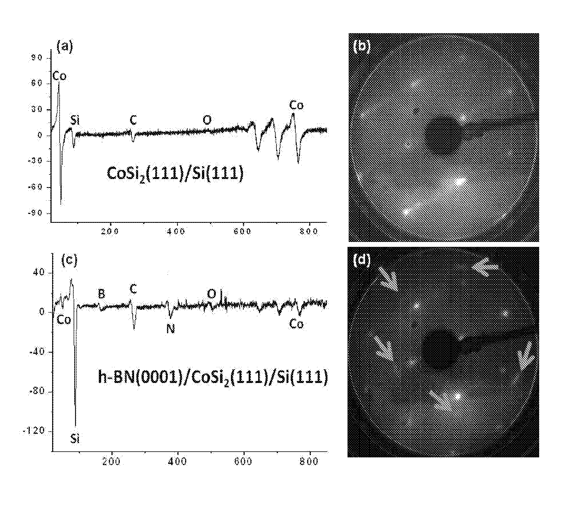
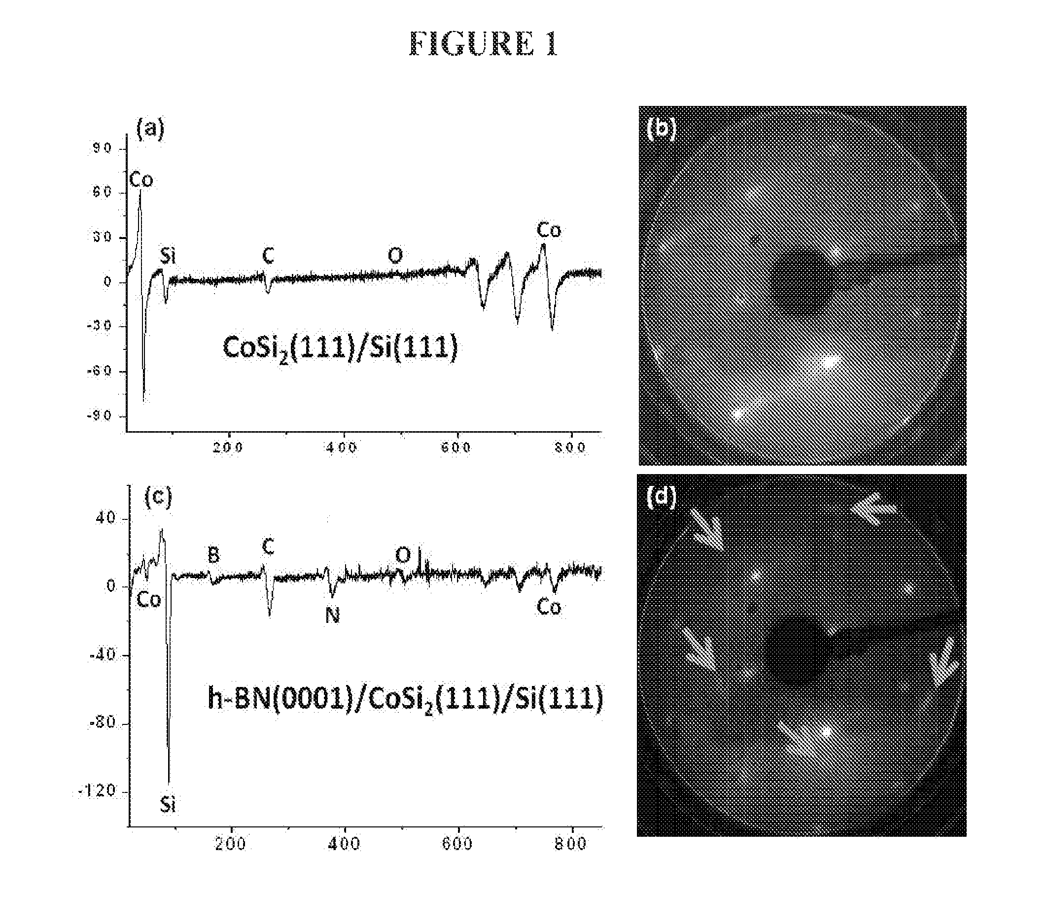
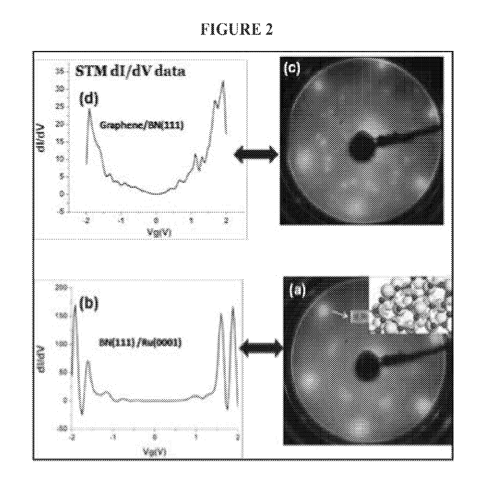
[0019]The data in Table I demonstrates that graphene / substrate interactions can profoundly affect graphene properties. Graphene was grown by CVD on a monolayer of h-BN(0001) formed by atomic layer deposition (ALD) on Ru(0001) [1]. Scanning tunneling spectroscopy (STS) and low energy electron diffraction (LEED) data showed significant orbital hybridization at the BN / Ru and grap...


PUM

PropertyMeasurementUnit
band gapaaaaaaaaaa
band gapaaaaaaaaaa
Néel temperatureaaaaaaaaaa

Abstract

We have demonstrated controlled growth of epitaxial h-BN on a metal substrate using atomic layer deposition. This permits the fabrication of devices such as vertical graphene transistors, where the electron tunneling barrier, and resulting characteristics such as ON-OFF rate may be altered by varying the number of epitaxial layers of h-BN. Few layer graphene is grown on the h-BN opposite the metal substrate, with leads to provide a vertical graphene transistor that is intergratable with Si CMOS technology of today, and can be prepared in a scalable, low temperature process of high repeatability and reliability.

Description

PRIORITY DATA AND INCORPORATION BY REFERENCE[0001]This application claims benefit of priority to U.S. Provisional Patent Application Ser. No. 61 / 668,629 filed Jul. 6, 2012 which is incorporated by reference in its entirety.BACKGROUND OF THE INVENTION[0002]1. Field of the Invention[0003]The present invention relates to controlled epitaxial growth of multiple layers of hexagonal boron nitride. The controlled growth multiple layers of hexagonal boron nitride (h-BN), coupled with the ability to deposit microscopically continuous layers of graphene thereon, paves the way for formation of vertically oriented graphene-based transistors. These and similar devices are also the subject of this patent application.[0004]2. Background of the Invention[0005]The direct growth of graphene films, by industrially practical and scalable methods, including CVD, PVD, or MBE, on dielectric substrates is a critical step towards the development of graphene charge- and spin-based devices. We have demonstrat...

Claims


Application Information

Patent Timeline
Patent Type & Authority Patents(United States)
IPC IPC(8): H01L29/78H01L29/66H01L29/267H01L29/16H01L29/76H01L21/02H01L29/04
CPCH01L29/7827H01L21/0254H01L21/0262H01L21/02425H01L21/02527H01L29/04H01L29/1606H01L29/267H01L29/66666H01L29/76H01L21/02381H01L21/02433H01L21/02458H01L21/02491H01L21/02502H01L21/02516
Inventor KELBER, JEFFRY
Owner UNIVERSITY OF NORTH TEXAS
Why Eureka
Try Eureka