Unlock instant, AI-driven research and patent intelligence for your innovation.

Self-bias emitter circuit

a self-bias, emitter circuit technology, applied in the direction of transducer details, magnetic restriction transducers, electrical transducers, etc., can solve the problem of increasing the cost of the emitter circuit, and achieve the effect of simplifying the operation of the emitter system and reducing operational costs

Active Publication Date: 2016-05-03
TURTLE BEACH
View PDF217 Cites 0 Cited by
  • Summary
  • Abstract
  • Description
  • Claims
  • Application Information

AI Technical Summary

Benefits of technology

The patent describes a self-bias emitter circuit that can receive a modulated or unmodulated AC carrier signal and convert it into a steady DC bias voltage without affecting the carrier information required for the emitter to emit parameter information. The circuit includes a transductor with an electromagnetic shielded pot core and a full-wave bridge rectifier that can convert the carrier signal into a DC voltage, which is then filtered to provide a steady voltage across the emitter. The circuit can also operate without the need for an auxiliary power supply, reducing operational costs and simplifying the system.

Problems solved by technology

To provide DC bias voltage, an auxiliary power supply can be operatively connected to the emitter, but this configuration can increase the cost of the emitter circuit while also implying the use of additional wires to connect the emitter with the auxiliary power supply.

Method used


Image

  • Self-bias emitter circuit
  • Self-bias emitter circuit
  • Self-bias emitter circuit

Examples


Embodiment Construction

[0033]In the following detailed description, reference is made to the accompanying drawings, which form a part hereof. In the drawings, which are not to scale or to proportion, similar symbols typically identify similar components, unless context dictates otherwise. The illustrative embodiments described in the detailed description, drawings and claims, are not meant to be limiting. Other embodiments can be used and / or and other changes can be made without departing from the spirit or scope of the present disclosure.

Definition of Terms

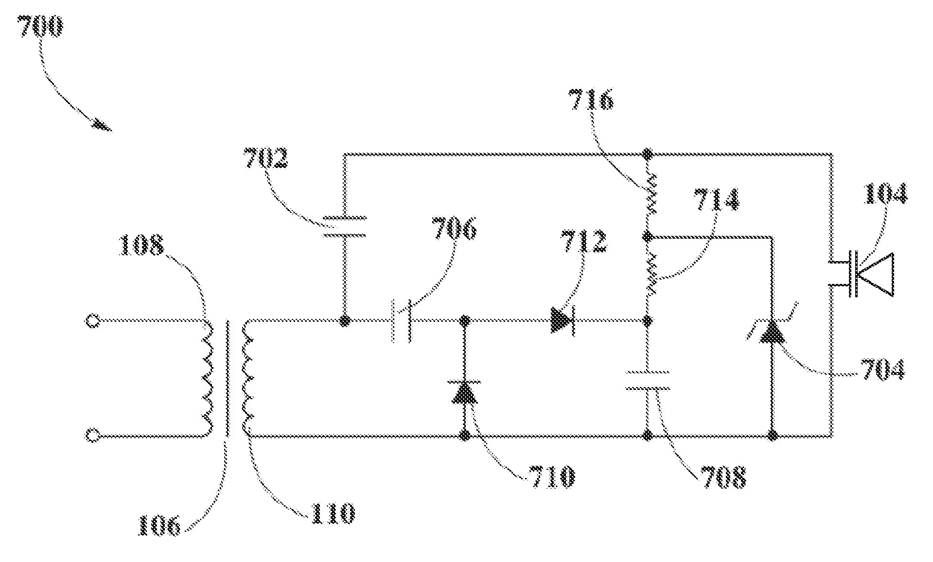
[0034]As used herein, “emitter” can refer to a device capable of emitting ultrasonic signals and that can be integrated in a self-bias emitter circuit.

[0035]As used herein, “self-bias emitter circuit” can refer to a circuit capable of transforming an input modulated or unmodulated AC carrier signal into a steady DC bias voltage.

[0036]As used herein, “DC bias voltage” can refer to a steady or constant DC voltage that can be obtained after rectification ...


PUM


Abstract

A emitter circuit for providing a bias voltage is disclosed. The emitter circuit can comprise an emitter. The emitter circuit can comprise a transductor that includes a primary winding and a secondary winding. The secondary winding can be operable to receive an alternating current (AC) carrier signal. The emitter circuit can comprise a voltage multiplier operable to receive the AC carrier signal from the secondary winding and generate a DC bias voltage. The emitter circuit can comprise a zener diode to limit an amplitude of the DC bias voltage applied across the emitter. The emitter circuit can comprise a filter capacitor operable to smooth the DC bias voltage applied across the emitter.

Description

PRIORITY CLAIM[0001]This is a continuation-in-part of U.S. patent application Ser. No. 14 / 667,542, filed Mar. 24, 2015, which is a continuation of U.S. patent application Ser. No. 13 / 917,315, filed Jun. 13, 2013, now issued as U.S. Pat. No. 8,988,911, all of which are hereby incorporated herein by reference in their entirety.BACKGROUND[0002]1. Field of the Invention[0003]The present disclosure relates generally to parametric loudspeakers for use in audio production, and more particularly, to emitter circuit configurations.[0004]2. Background Information[0005]A new form of emitters can include a film made of plastic materials such as kapton, mylar, and polypropylene, among others. The upper side of this film can be laminated with a conductive material such as copper, nickel, aluminum, or gold.[0006]The emitter can also include a back plate or stator which can be configured to exhibit a plurality of microscopic slots or pits arranged in a specific pattern. The lower side of the stator...

Claims


Application Information

Patent Timeline
Patent Type & Authority Patents(United States)
IPC IPC(8): H02M7/06H04R3/00
CPCH04R3/00H02M7/06H04R2217/03
Inventor WOOD, STEPHENNORRIS, ELWOOD
Owner TURTLE BEACH