All-optical NAND/NOT/AND/OR logic gates based on combined brillouin gain and loss in an optical fiber

a logic gate and optical fiber technology, applied in the field of optical logic gates, can solve the problems of slowing down the operation of all-optical logic gates, falling victim to additional noise, and limited soa-based techniques

Active Publication Date: 2016-05-10
WILLIAMS DAISY
View PDF2 Cites 2 Cited by
  • Summary
  • Abstract
  • Description
  • Claims
  • Application Information

AI Technical Summary

Benefits of technology

[0033]the high power of the input signal and the second high power of the second input signal yields the power of the output signal below another low threshold, wherein the another low threshold is lower than the another high threshold.
[0136]the high power of the input signal and the second high power of the second input signal yields the power of the output signal below another low threshold, wherein the another low threshold is lower than the another high threshold.

Problems solved by technology

SOA-based techniques are often limited by the carrier's recovery time, which, in turn, slows down the operation of the all-optical logic gate.
In addition, these techniques often require the use of multiple SOAs to achieve functional all-optical logic gates, and fall victim to additional noise such as spontaneous emission noise as described for example in Wang, J., Sun, J., Sun, Q., “Experimental observation of a 1.5 μm band wavelength conversion and logic NOT gate at 40 Gbit / s based on sum-frequency generation,” Optics Letters, 2006 vol 31: 1711-3; and Wang, J., Sun, J., Sun, Q., “Proposal for all-optical switchable OR / XOR logic gates using sum-frequency generation,” IEEE Photonics Technology Letters, 2007, vol 19: 541-3.
However, long fiber lengths introduce polarization instabilities, which is one limitation of the aforementioned technique.
Since polarization rotation is necessary in the papers of C. Yu cited above, presence of birefringence is another limitation of the technique, which may cause polarization mode dispersion (PMD) of the optical signal.

Method used


Image

  • All-optical NAND/NOT/AND/OR logic gates based on combined brillouin gain and loss in an optical fiber
  • All-optical NAND/NOT/AND/OR logic gates based on combined brillouin gain and loss in an optical fiber
  • All-optical NAND/NOT/AND/OR logic gates based on combined brillouin gain and loss in an optical fiber

Examples


embodiment 1

Configuration I (Embodiment 1)

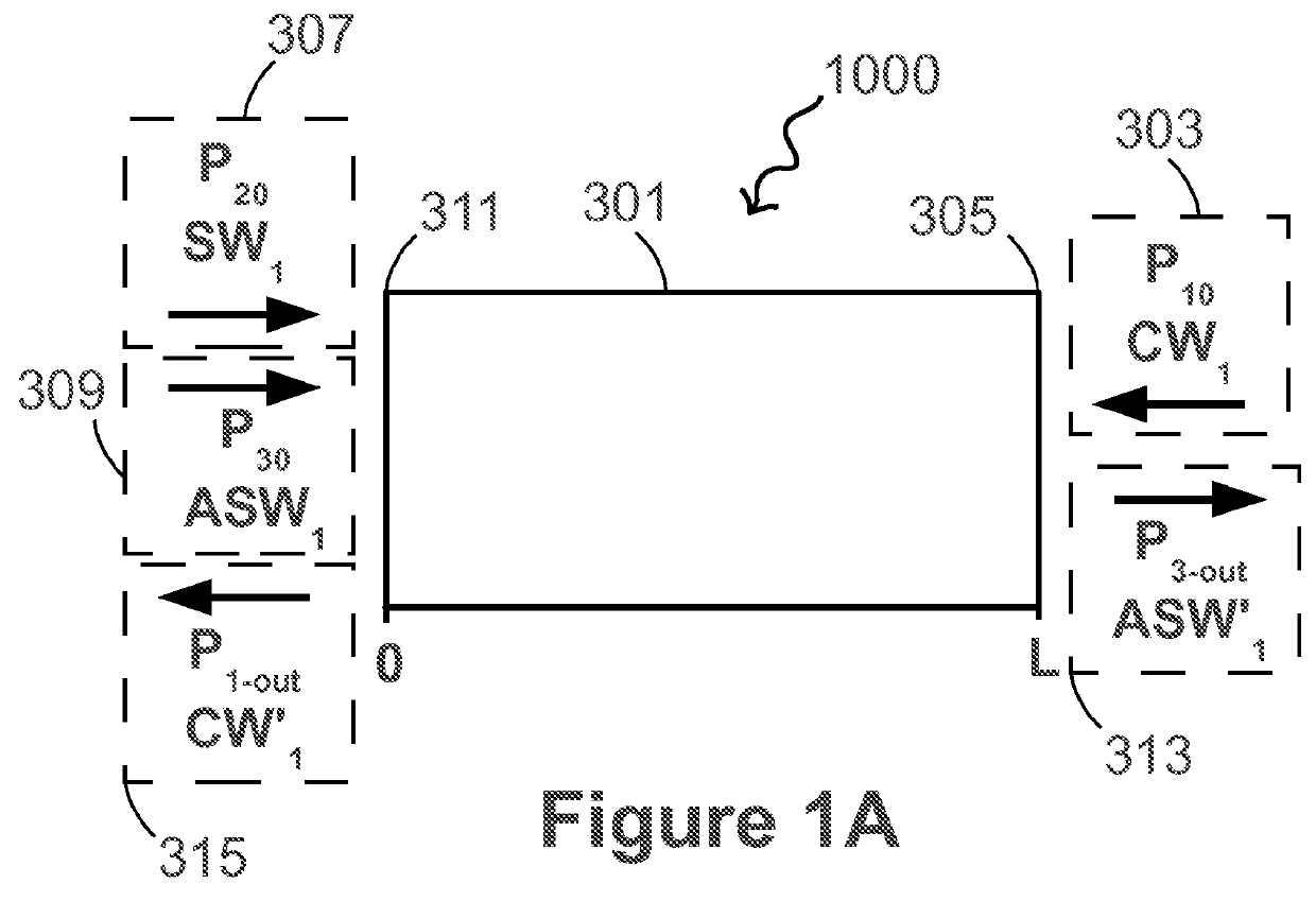
[0279]The Configuration I of the NAND gate, or NAND I, may be formed using the schematic arrangement 1000 from FIG. 1A. P10 (CW1) 303 is used as an input signal, injected into the opposite end of the optical fiber 305, and P20 (SW1) 307 is used as a second input signal, injected into the one end 311 of the optical fiber 301, P30 (ASW1) 309 is used as the reference signal, injected into the one end 311 of the optical fiber 301, and the output ASW power, P3-out (ASW′1) 313 is used as the output signal, exiting the opposite end 305 of the optical fiber 301.

[0280]

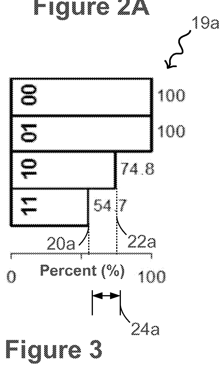
TABLE 1NAND I gate, L = 2300 m, P30 = 40 mW for all logical inputsP10P20P3-out001(0.1 mW)(0.1 mW)(25.1 mW)011(0.1 mW) (10 mW)(25.0 mW)101 (10 mW)(0.1 mW)(7.48 mW)110 (10 mW) (10 mW)(5.47 mW)

[0281]A power of 0.1 mW (low power) was assigned a logical value of ‘0’, while a power of 10 mW (high power) was assigned a logical input value of ‘1’. As shown in Table 1, the logical output ‘1’ is represented ...

embodiment 2

Configuration II (Embodiment 2)

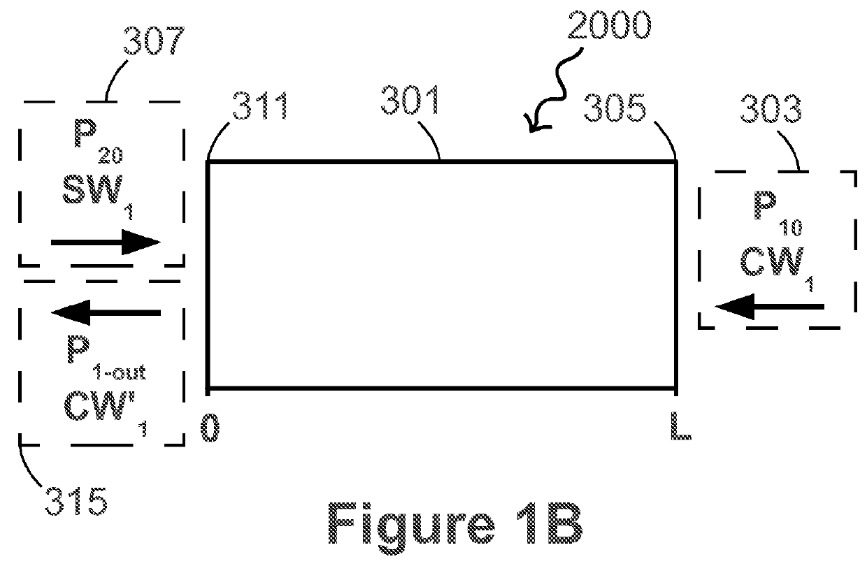
[0285]The Configuration II of the NAND II gate, or NAND II, may be formed using the schematic arrangement 1000 from FIG. 1A. In comparison with NAND I of FIG. 3 and Table 1, in NAND II a reference signal P30 (ASW1) 309 is also varied for each logical input.

[0286]The truth table for NAND II is shown in Table 2, and a NAND II switching contrast bar graph 19b is shown in FIG. 4. The NAND II tolerance 24b between the low threshold of NAND II 20b (35.8%) and high threshold of NAND II 22b (87.8%), is 52.7%, and is larger than the NAND I tolerance 24a. The fiber length for NAND II is 500 m. The trade-off is the required change in ASW input power, P30 (ASW1) 309, for the “1 0” logical input, as well as the need for additional information, pertaining to this power change. As such, some additional calibrations would be needed to realize the function of this logic gate, since it would require amplitude modulation of the output ASW, P′30 (ASW′1) 313, (output signa...

embodiment 3

Configuration III (Embodiment 3)

[0289]The Configuration III of the NAND III gate, or NAND III, may be formed using the schematic arrangement 1000 from FIG. 1A. In comparison with NAND I of FIG. 3 and Table 1, in NAND III, a detuning of the second input signal P20 (SW1) 307, or the reference signal P30 (ASW1) 309 is implemented for each logical input.

[0290]FIGS. 6A-6D depict the P3-out (ASW′1) 313 spectra. FIG. 6A shows a spectrum for the output signal (ASW) for logical input ‘0 0’ with ASW being detuned; FIG. 6B shows a spectrum for the output signal (ASW) for logical input ‘0 1’ with ASW being detuned; FIG. 6C shows a spectrum for the output signal (ASW) for logical input ‘1 0’ with ASW being detuned; and FIG. 6D shows a spectrum for the output signal (ASW) for logical input ‘1 1’ with SW being detuned.

[0291]We see that it is possible to optimize the output signal by detuning the frequency of either the SW, P20 (SW1) 307, or ASW, P30 (ASW1) 309. For each case in FIGS. 6A-6D, a detu...


PUM

PropertyMeasurementUnit
lengthaaaaaaaaaa
powersaaaaaaaaaa
core radiusaaaaaaaaaa

Abstract

A combined Brillouin gain and loss process has been created in a polarization maintaining optical fiber to realize all-Optical NAND / NOT / AND / OR logic gates in the frequency domain. A model describing the interaction of a Stokes, anti-Stokes and continuous wave, and two acoustic waves inside a fiber, ranging in length from 350 m-2300 m, was used to theoretically model the gates. Through the optimization of the gain and loss process, switching contrasts of 20-88% have been achieved, under different configurations. Experimental setups for NAND / NOT / AND / OR optical logic gates have been described. A method and system for designing the all-optical logic gates have been also provided.

Description

RELATED APPLICATIONS[0001]The present patent application claims benefit from the US provisional application to Daisy Williams et al. Ser. No. 61 / 710,558 filed on Oct. 5, 2012 entitled “All-Optical NAND / NOT / AND / OR Logic Gates based on Combined Brillouin Gain and Loss in an Optical Fiber”, entire contents of which are incorporated herein by reference.FIELD OF THE INVENTION[0002]The present invention related to optical logic gates, and in particular to all-optical logic gates based on stimulated Brillouin scattering (SBS) in optical fibers.BACKGROUND OF THE INVENTION[0003]In view of the speed limitations inherent in electronic circuits, all-optical data processing devices have become the focus of many research efforts. One category of such devices is the all-optical logic gate, which is deemed to be a main component in future integrated photonic circuits.[0004]Some established techniques for achieving functional all-optical logic gates include: 1) use of integrated fiber based Mach-Zeh...

Claims


Application Information

Patent Timeline
Patent Type & Authority Patents(United States)
IPC IPC(8): G06E3/00G02F3/00G02F3/02
CPCG02F3/026
Inventor WILLIAMS, DAISYBAO, XIAOYICHEN, LIANG
Owner WILLIAMS DAISY
Why Eureka
Try Eureka