CMOS image sensor unit and method for fabricating the same

a sensor unit and image technology, applied in the field of image sensor units, can solve the problems of image lag, difficult to completely transfer the charge generated in the photodiode to the floating drain region, and limited dynamic range of image sensing, so as to reduce the dark current, increase the dynamic range, and reduce the effect of fill factor

Active Publication Date: 2016-07-12
POWERCHIP SEMICON MFG CORP
View PDF6 Cites 3 Cited by
  • Summary
  • Abstract
  • Description
  • Claims
  • Application Information

AI Technical Summary

Benefits of technology

[0008]The invention provides a CMOS image sensor unit capable of increasing the dynamic range as well as reducing the dark current, without reducing the fill factor.

Problems solved by technology

However, for the capacitance (CPD) of the entire photodiode region is larger than that (CFD) of the floating drain region, charges generated in the photodiode are difficult to totally transfer to the floating drain region during the period of switching on the transfer transistor.
Thus, after the transfer transistor is switched off, some charges remain in the photodiode and lead to an image lag.
Therefore, the dynamic range of image sensing is limited.
The leakage existing in the hetero junction easily causes a dark current during the image sensing, so that noise is formed during signal sensing.

Method used


Image

  • CMOS image sensor unit and method for fabricating the same
  • CMOS image sensor unit and method for fabricating the same
  • CMOS image sensor unit and method for fabricating the same

Examples


Embodiment Construction

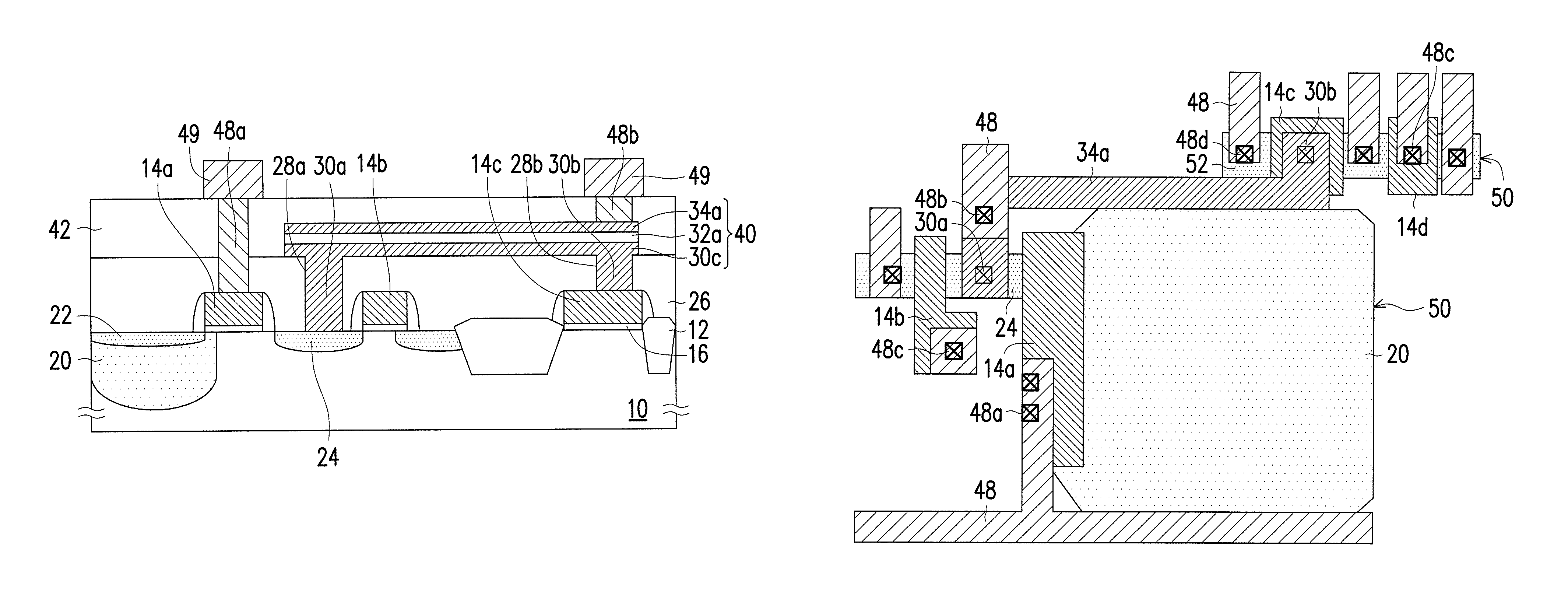
[0018]An embodiment is provided to illustrate the invention, but is not intended to limit the same. For instance, even though in this embodiment a 4-transistor (4T) CMOS image sensor unit including a transfer gate, a reset gate, a source follower gate and a row select gate (RS gate) is described, other type of CMOS image sensor unit may be applied as long as having the base structure containing a photodiode, a transfer gate, a reset gate, a floating drain region and a source follower gate.

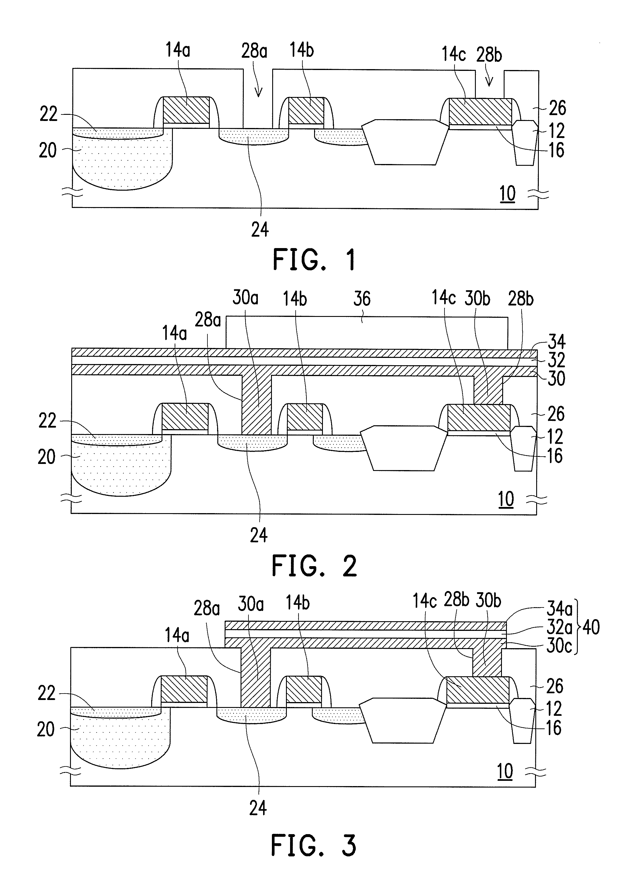
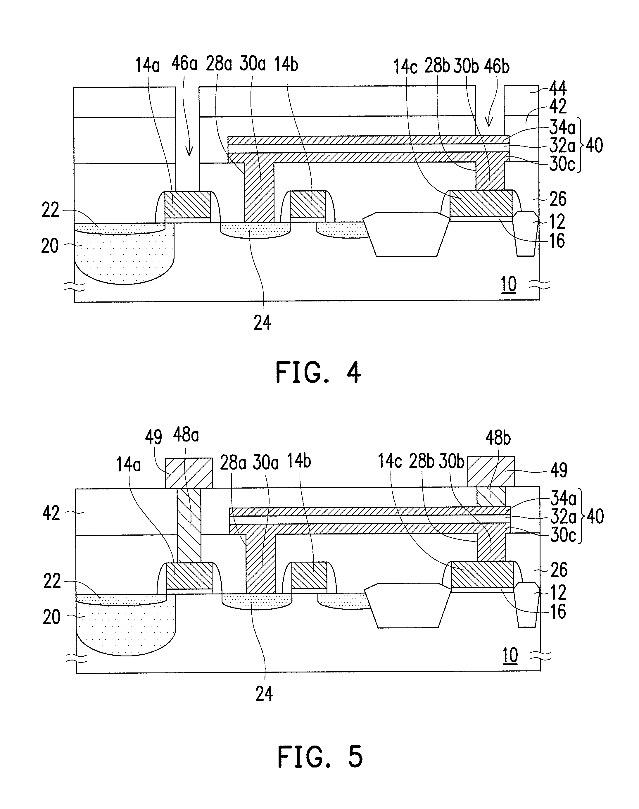
[0019]FIGS. 1 to 5 are cross-sectional views showing a method for fabricating an image sensor unit according to an embodiment of the invention, wherein FIG. 5 is a cross-sectional view of the image sensor unit of the embodiment.

[0020]Referring to FIG. 1, a semiconductor substrate 10 is provided, which includes, for example, doped monocrystalline silicon, and has a conductivity type of, for example, P-type. An isolation layer 12 is formed on the semiconductor substrate 10 to define an active region,...


PUM


Abstract

A CMOS image sensor unit and a method for fabricating the same are described. The image sensor unit includes a photodiode, a transfer gate, a reset gate, a source follower gate, a floating drain region between the transfer gate and the reset gate, and a PIP capacitor. The lower poly-Si electrode of the PIP capacitor is electrically connected with the floating drain region and the source follower gate to also serve as an interconnect between the floating drain region and the source follower gate. The fabrication method includes forming contact plugs on the floating drain region and the source follower gate, and then forming a PIP capacitor whose lower poly-Si electrode is connected with each contact plug.

Description

CROSS-REFERENCE TO RELATED APPLICATION[0001]This application claims the priority benefits of Taiwan Application serial no. 104112060, filed on Apr. 15, 2015. The entirety of the above-mentioned patent application is hereby incorporated by reference herein and made a part of this specification.BACKGROUND[0002]1. Field of the Invention[0003]The invention is directed to an image sensor unit, and more particularly to a CMOS image sensor unit and a method for fabricating the same.[0004]2. Description of Related Art[0005]A typical CMOS image sensor unit includes a photodiode (PD), a transfer gate, a reset gate, a source follower gate, and a floating drain region (FD) between the transfer gate and the reset gate. The floating drain region is electrically connected with the source follower gate through a metal interconnect. During the operation, the charges generated from the photodiode having received a light signal flows to the floating drain region through the channel controlled by the t...

Claims


Application Information

Patent Timeline
Patent Type & Authority Patents(United States)
IPC IPC(8): H01L27/00H01L27/146
CPCH01L27/14643H01L27/14612H01L27/14689H01L27/14609
Inventor CHUNG, CHIH-PINGCHEN, MING-WEICHEN, MIN-HUIHO, MING-YU
Owner POWERCHIP SEMICON MFG CORP
Why Eureka
Try Eureka