Light-emitting device comprising an organic compound

a light-emitting device and organic compound technology, applied in the direction of organic semiconductor devices, solid-state devices, semiconductor devices, etc., can solve the problems of chemical instability of the host material, and achieve the effects of high emission efficiency, long life and high reliability

Active Publication Date: 2016-07-12
SEMICON ENERGY LAB CO LTD
View PDF58 Cites 12 Cited by
  • Summary
  • Abstract
  • Description
  • Claims
  • Application Information

AI Technical Summary

Benefits of technology

[0007]An object of one embodiment of the present invention is to provide a chemically stable light-emitting device. Another object of one embodiment of the present invention is to provide a light-emitting device having high emission efficiency. Another object of one embodiment of the present invention is to provide a highly reliable light-emitting device. Another object of one embodiment of the present invention is to provide a light-emitting device in which image burn-in is unlikely to occur. Another object of one embodiment of the present invention is to provide a light-emitting device in which delayed light emission is performed. Another object of one embodiment of the present invention is to provide a novel light-emitting device. Another object of one embodiment of the present invention is to provide an excellent light-emitting device.
[0016]Note that in each of the above structures, an organic compound whose T1 level is lower than that of the guest material can be used as the host material; thus, the light-emitting element can be fabricated without using a chemically unstable organic compound as the host material even.
[0017]In any of the above structures, the host material is preferably selected such that the guest material such that the T1 level of the host material is lower than that of the guest material, and the difference in T1 level is greater than or equal to 0 eV and less than or equal to 0.2 eV. Accordingly, a chemically stable host material can be used without decreasing emission efficiency, leading to a long-lifetime light-emitting element.
[0019]A light-emitting element of one embodiment of the present invention can have high emission efficiency. A light-emitting element of one embodiment of the present invention can have a long lifetime by including a chemically stable host material in a light-emitting layer. A light-emitting device of one embodiment of the present invention can have high reliability by including the light-emitting element. An electronic device and a lighting device of one embodiment of the present invention can have high reliability by including the light-emitting device.

Problems solved by technology

However, in the case where a phosphorescent compound having high emission energy (e.g., a blue phosphorescent compound) is used as a guest material, the T1 level of a host material needs to be higher than that in the case where a phosphorescent compound having lower emission energy (e.g., a green or red phosphorescent compound) is used as a guest material; thus, there is a problem in that the host material becomes chemically unstable.

Method used


Image

  • Light-emitting device comprising an organic compound
  • Light-emitting device comprising an organic compound
  • Light-emitting device comprising an organic compound

Examples


embodiment 1

(Embodiment 1)

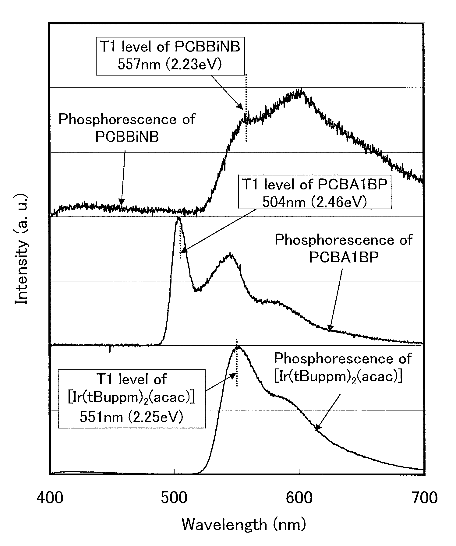
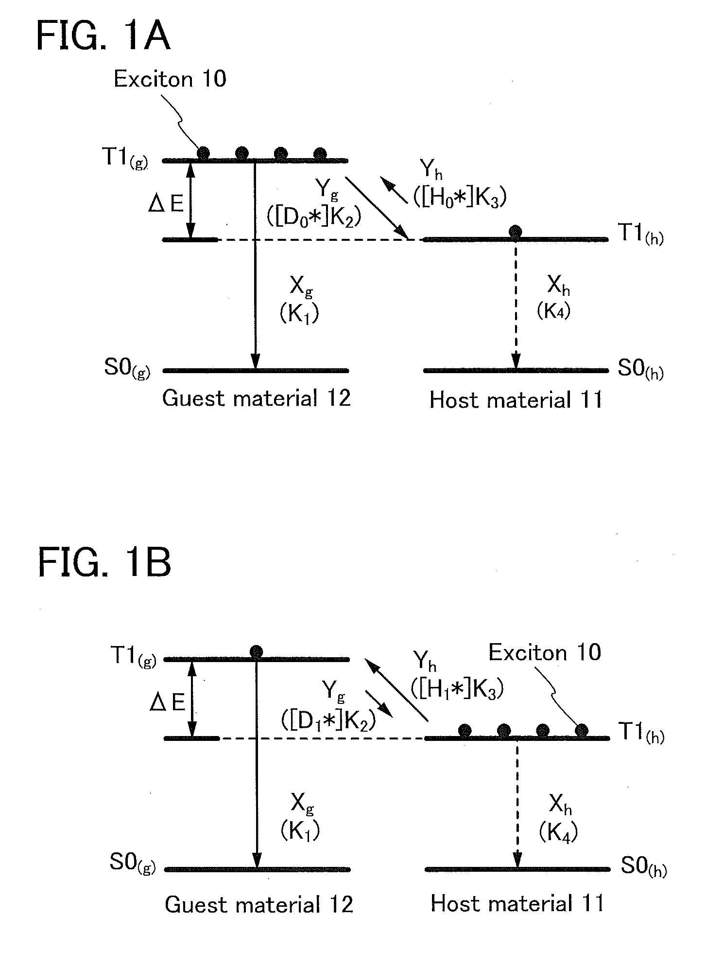
[0046]In this embodiment, described are a concept and a specific structure of a light-emitting element of one embodiment of the present invention. The light-emitting element includes a host material capable of remaining chemically stable even if a phosphorescent compound having high emission energy is used as a guest material.

[0047]In a light-emitting element of one embodiment of the present invention, a light-emitting layer is provided between a pair of electrodes, and the light-emitting layer contains at least a host material and a guest material (the exciton concentration is in a range where concentration quenching does not occur). The relation between the relative emission intensity and the emission time of light emission obtained from these materials (e.g., photoluminesence (PL) by photoexcitation or electroluminescence (EL) by electric field excitation) is represented by a multicomponent decay curve. The relative emission intensity of the slowest component of the...

embodiment 2

(Embodiment 2)

[0069]In this embodiment, an example of a light-emitting element of one embodiment of the present invention is described with reference to FIG. 3.

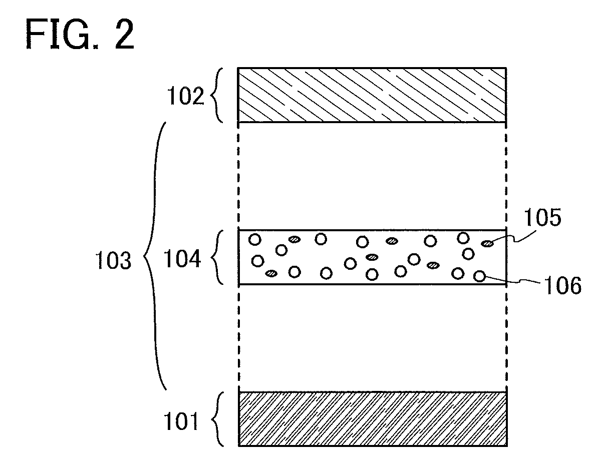
[0070]In the light-emitting element described in this embodiment, as illustrated in FIG. 3, an EL layer 203 including a light-emitting layer 206 is provided between a pair of electrodes (a first electrode (anode) 201 and a second electrode (cathode) 202), and the EL layer 203 includes a hole-injection layer 204, a hole-transport layer 205, an electron-transport layer 207, an electron-injection layer 208, and the like in addition to the light-emitting layer 206.

[0071]As in the light-emitting element described in Embodiment 1, the light-emitting layer 206 contains at least the first organic compound 209 serving as a host material and the second organic compound 210 serving as a guest material. Since the same substances described in Embodiment 1 can be used as the first organic compound 209 and the second organic compound 210, a...

embodiment 3

(Embodiment 3)

[0088]In this embodiment, as one embodiment of the present invention, a light-emitting element (hereinafter referred to as tandem light-emitting element) in which a charge generation layer is provided between a plurality of EL layers is described.

[0089]The light-emitting element described in this embodiment is a tandem light-emitting element including a plurality of EL layers (a first EL layer 302(1) and a second EL layer 302(2)) between a pair of electrodes (a first electrode 301 and a second electrode 304) as illustrated in FIG. 4A.

[0090]In this embodiment, the first electrode 301 functions as an anode, and the second electrode 304 functions as a cathode. Note that the first electrode 301 and the second electrode 304 can have structures similar to those described in Embodiment 2. In addition, all or any of the plurality of EL layers (the first EL layer 302(1) and the second EL layer 302(2)) may have structures similar to those described in Embodiment 2. In other word...


PUM


Abstract

A light-emitting element of the present invention can have sufficiently high emission efficiency with a structure including a host material being able to remain chemically stable even if a phosphorescent compound having higher emission energy is used as a guest material. The relation between the relative emission intensity and the emission time of light emission obtained from the host material and the guest material contained in a light-emitting layer is represented by a multicomponent decay curve. The relative emission intensity of the slowest component of the multicomponent decay curve becomes 1 / 100 for a short time within a range where the slowest component is not interfered with by quenching of the host material (the emission time of the slowest component is preferably less than or equal to 15 μsec); thus, sufficiently high emission efficiency can be obtained.

Description

TECHNICAL FIELD[0001]The present invention relates to an object, a method, a manufacturing method, a process, a machine, manufacture, or a composition of matter. In particular, the present invention relates to, for example, a semiconductor device, a display device, a light-emitting device, a power storage device, a driving method thereof, or a manufacturing method thereof. Specifically, one embodiment of the present invention relates to a light-emitting element in which an organic compound capable of providing light emission by application of an electric field is provided between a pair of electrodes, and also relates to a light-emitting device, an electronic device, and a lighting device including such a light-emitting element.BACKGROUND ART[0002]A light-emitting element using an organic compound as a luminous body, which has features such as thinness, lightness, high-speed response, and DC drive at low voltage, is expected to be applied to a next-generation flat panel display. In ...

Claims


Application Information

Patent Timeline
Patent Type & Authority Patents(United States)
IPC IPC(8): H01L51/50H01L51/00
CPCH01L51/5016H01L51/0059H01L51/0072H01L51/0074H01L51/0085H01L2251/5384H01L2251/55H10K85/631H10K85/6576H10K85/6572H10K85/342H10K50/11H10K2101/10H10K2101/90H10K2101/00H01L2924/12044H10K50/12H10K50/121H10K85/633H10K85/636H10K59/12H10K85/615H10K2102/361
Inventor WATABE, TAKEYOSHISEO, SATOSHI
Owner SEMICON ENERGY LAB CO LTD
Why Eureka
Try Eureka