Guided wave applicator with non-gaseous dielectric for plasma chamber

a technology of non-gaseous dielectric and applicator, which is applied in waveguide devices, waveguide types, waveguides, etc., can solve the problems of difficult scaling up to plasma chambers for processing workpieces, difficult to achieve good spatial uniformity of plasma density in a large chamber, and impair the spatial uniformity of plasma produced in the plasma chamber. achieve the effect of convenient and inexpensive operation

Inactive Publication Date: 2016-07-19
APPLIED MATERIALS INC
View PDF29 Cites 191 Cited by
  • Summary
  • Abstract
  • Description
  • Claims
  • Application Information

AI Technical Summary

Benefits of technology

[0016]Advantageously, because the volume of the waveguide dielectric is composed of non-gaseous material, there is no need to provide a vacuum seal or to maintain a pressure differential between the interior of the guided wave applicator and the low pressure interior of the plasma chamber. Consequently, the guided wave applicator readily and inexpensively can be fabricated with as great a length as desired for use in fabricating large electronic devices such as solar panels or flat panel displays.

Problems solved by technology

Consequently, a disadvantage of this type of design is that it is difficult to achieve good spatial uniformity of the plasma density in a large chamber because the plasma density tends to be lower near the center of the chamber than near the surrounding chamber wall.
A disadvantage of this type of design is that it is difficult to scale up to plasma chambers for processing workpieces that are several meters wide because it is difficult and expensive to manufacture a dielectric wall that is several meters long, can sustain the aforesaid pressure differential over its entire surface, and can withstand thermal shock from the high temperatures within a plasma chamber.
This can impair the spatial uniformity of the plasma produced within the plasma chamber.

Method used


Image

  • Guided wave applicator with non-gaseous dielectric for plasma chamber
  • Guided wave applicator with non-gaseous dielectric for plasma chamber
  • Guided wave applicator with non-gaseous dielectric for plasma chamber

Examples


Embodiment Construction

1. Basic Features of Invention

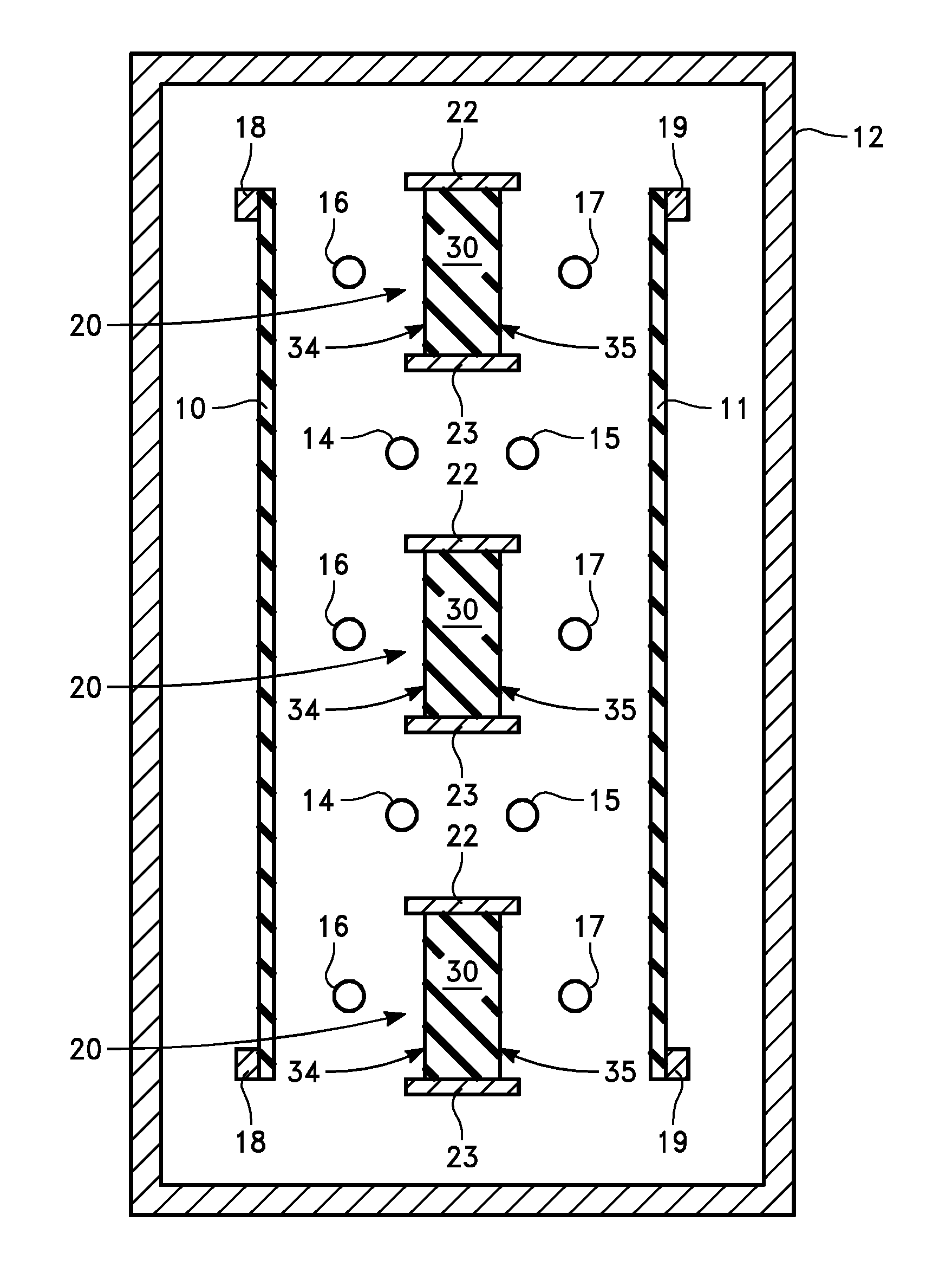
[0027]FIG. 1 is a sectional top view of one embodiment of a plasma chamber according to the invention.

[0028]In the FIG. 1 embodiment, first and second workpiece supports 18, 19 respectively support first and second flat workpieces at respective workpiece positions 10, 11 in a vertical orientation within a plasma chamber. In alternative embodiments, the workpieces can be oriented horizontally or can be tilted at an acute angle. Examples of workpieces that can be processed in the plasma chamber are a glass substrate for fabrication of flat panel displays or a silicon substrate for fabrication of semiconductor circuits or solar cells.

[0029]The plasma chamber has a chamber wall 12 that is electrically grounded and that surrounds the chamber interior. One or more process gases are supplied to the interior of the plasma chamber through one or more process gas conduits 14-17. In the illustrated embodiment, the process gas conduits are vertically oriented cylin...


PUM

PropertyMeasurementUnit
electrical poweraaaaaaaaaa
electrically conductiveaaaaaaaaaa
volumeaaaaaaaaaa

Abstract

A guided wave applicator comprising two electrically conductive waveguide walls and a waveguide dielectric. The volume of the waveguide dielectric is composed of non-gaseous dielectric material and is positioned between the two waveguide walls. The waveguide dielectric includes first and second longitudinal ends and includes first, second, third and fourth sides extending longitudinally between the two longitudinal ends. The first waveguide wall is positioned so that it covers the first side of the waveguide dielectric, and the second waveguide wall is positioned so that it covers the second side of the waveguide dielectric. In operation, electrical power can be supplied to one or both longitudinal ends of the waveguide dielectric, whereby the power can be coupled to a plasma through the exposed sides of the waveguide dielectric.

Description

CROSS REFERENCE TO RELATED APPLICATION[0001]This patent application claims the benefit of U.S. Provisional Application No. 61 / 437,007 filed Jan. 28, 2011.TECHNICAL FIELD[0002]The invention relates generally to guided wave applicator methods and apparatus useful for forming a plasma discharge in a process chamber for fabricating electronic devices such as semiconductors, displays and solar cells. The invention relates more specifically to a guided wave applicator comprising a non-gaseous dielectric having two opposite sides that are not covered by a metal waveguide wall.BACKGROUND ART[0003]Plasma chambers commonly are used to perform processes for fabricating electronic devices such as semiconductors, displays and solar cells. Such plasma fabrication processes include chemical vapor deposition of semiconductor, conductor or dielectric layers on the surface of a workpiece or etching of selected portions of such layers on the workpiece surface.[0004]A plasma commonly is formed in a pla...

Claims


Application Information

Patent Timeline
Patent Type & Authority Patents(United States)
IPC IPC(8): H01P3/16H01J37/32H05H1/46H01L21/02
CPCH01P3/16H01J37/32229H01L21/02H01L21/02104H05H1/46H05H2001/4622H05H1/4622
Inventor KUDELA, JOZEFTANAKA, TSUTOMUSORENSEN, CARL A.ANWAR, SUHAILWHITE, JOHN M.
Owner APPLIED MATERIALS INC
Why Eureka
Try Eureka