Dual-mode memory devices and methods for operating same

a memory device and dual-mode technology, applied in the direction of solid-state devices, semiconductor devices, instruments, etc., can solve the problems of block erase operation requirements, circuitry implementation limitations, and limited flexibility in the layout of integrated circuits, etc., and achieve the effect of low leakage and fast transition times

Active Publication Date: 2016-10-04
MACRONIX INT CO LTD
View PDF28 Cites 0 Cited by
  • Summary
  • Abstract
  • Description
  • Claims
  • Application Information

AI Technical Summary

Benefits of technology

This patent describes a memory structure that can act in both p-channel and n-channel modes, allowing for fast transition times and low leakage. The structure includes bias circuitry to selectively induce the formation of holes or electrons in target memory cells, depending on the mode of operation. This results in a flash memory with the capability for bit erase and bit program operations, and also helps to suppress leakage current during operation.

Problems solved by technology

This can limit flexibility in the layout of an integrated circuit, and in the implementation of circuitry utilizing the transistors.
Further limitations in many types of prior art flash memory technologies relate to the requirement for block erase operations.
Because of the reliance on block erase, the complexity of the required operations and the amount of required time for writing data in random addresses of the flash memory are increased.
Also, the dual-mode memory structure can be operated with very steep subthreshold slope, resulting in fast transition times and low leakage.

Method used


Image

  • Dual-mode memory devices and methods for operating same
  • Dual-mode memory devices and methods for operating same
  • Dual-mode memory devices and methods for operating same

Examples


Embodiment Construction

[0048]A detailed description is provided with reference to the FIGS. 1-31.

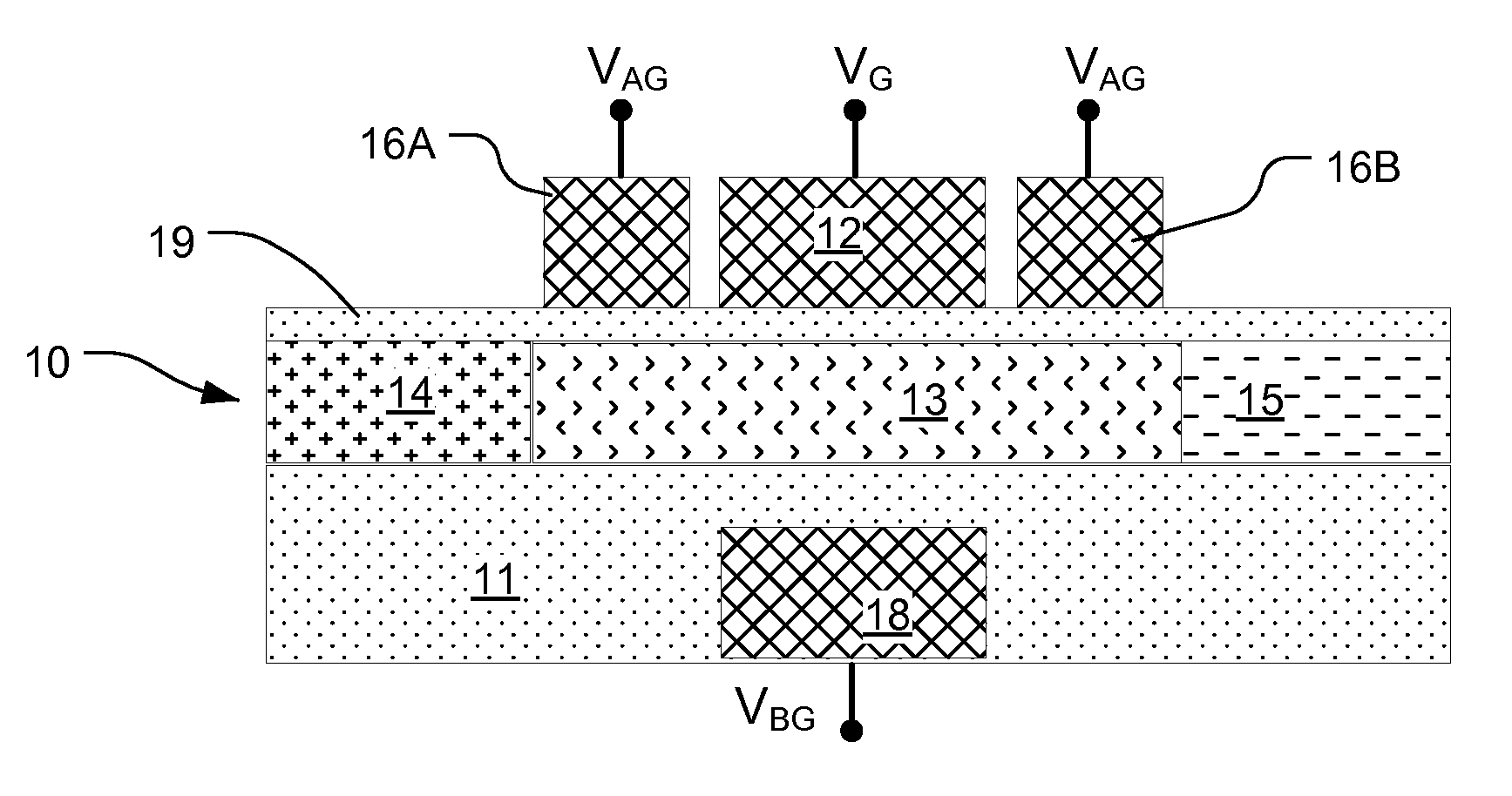
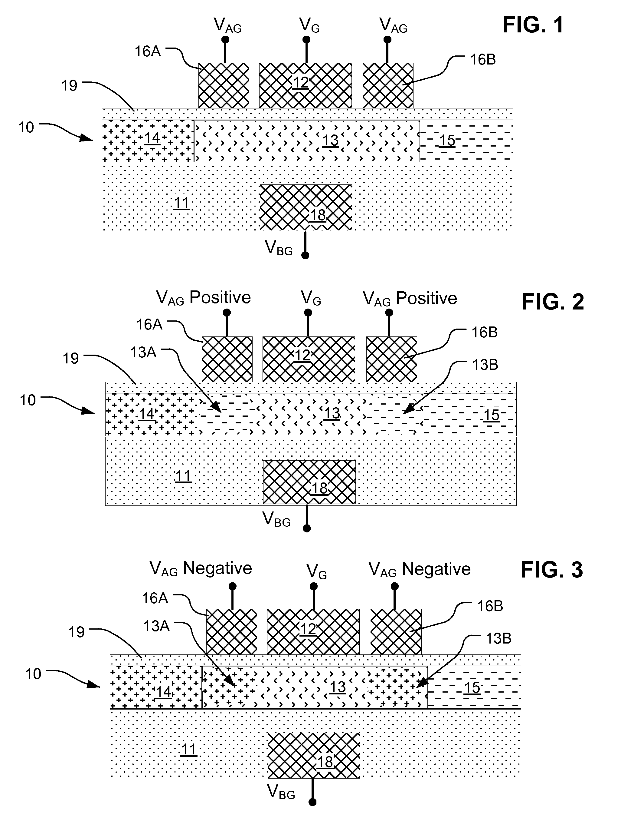
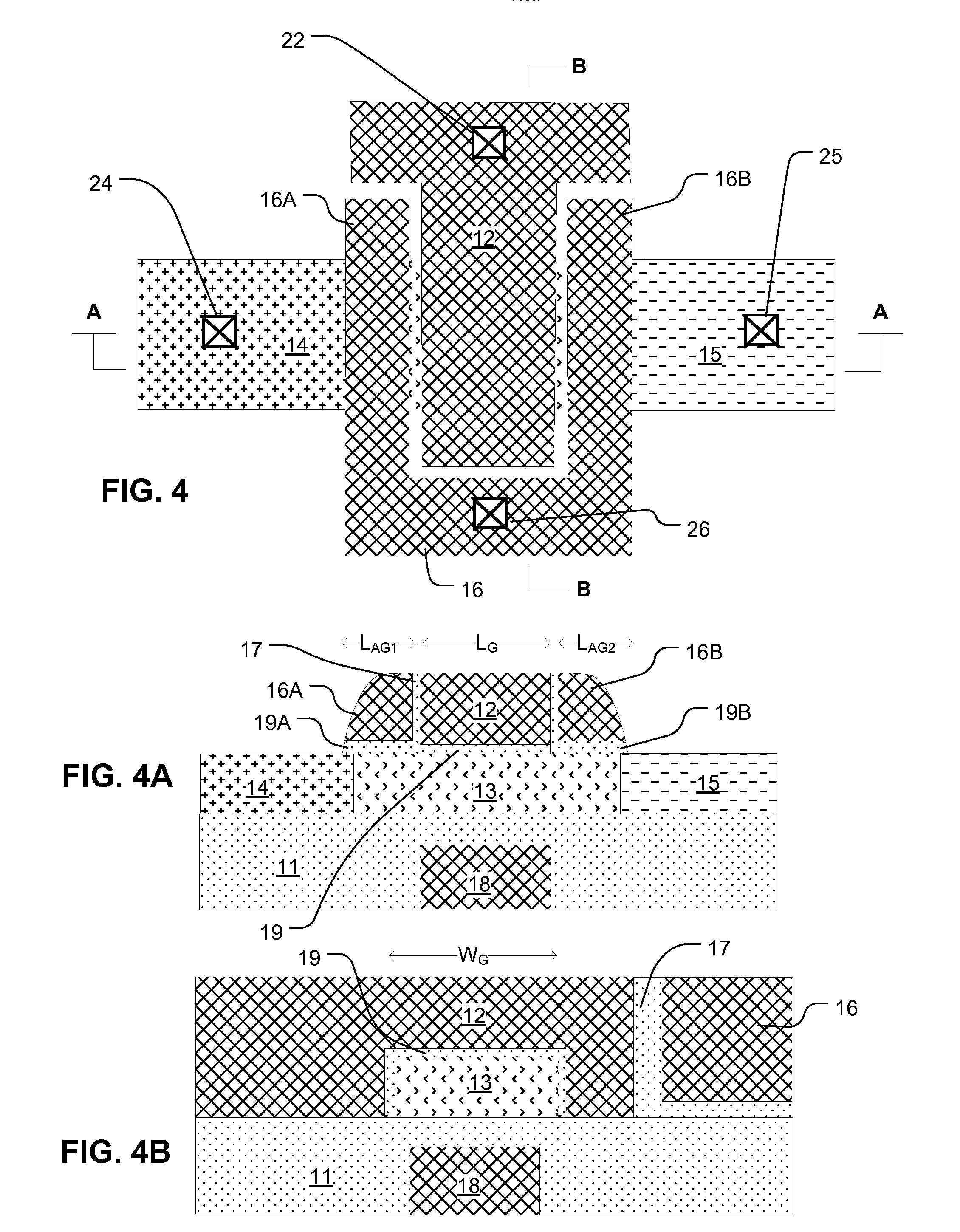
[0049]FIG. 1 is a cross-section of a dual-mode transistor structure taken along the channel length dimension. The transistor structure includes a semiconductor body 10 that has a channel region 13, a first terminal region 14 having p-type doping and a second terminal region 15 having n-type doping. In the channel region 13, the semiconductor body can be undoped, or have a doping profile that is configured for a channel according to a particular application of the device. It can be preferred for some applications that the channel region 13 be configured for fully depleted operation, such as by having a width that is less than the maximum depletion width. The semiconductor body 10 is disposed on an insulator 11. The structure can comprise a silicon-on-insulator SOI substrate.

[0050]A gate structure 12 overlies the channel region 13 of the semiconductor body 10. A first assist gate 16A is disposed on a first side ...


PUM


Abstract

A memory structure comprises a semiconductor strip having a multi-gate channel region, the p-type terminal region adjacent a first side of the channel region and an n-type terminal region adjacent the second side of the channel region. A plurality of word lines is arranged to cross the semiconductor strip at cross points in the channel region. The bit line is coupled to a first end of the semiconductor strip, and a reference line is coupled to a second end of the semiconductor strip. Charge storage structures are disposed between the word lines in the plurality word lines and the channel region of the semiconductor strip, whereby memory cells are disposed in series along the semiconductor strip between the bit line and the reference line. Biasing unselected word lines can be used to select n-channel or p-channel modes in a single selected cell for read, program or erase.

Description

[0001]Benefit of U.S. Provisional Patent Application No. 61 / 831,630, filed 6 Jun. 2013, entitled “Operation Methods for Dual-Channel 3D NAND Flash,” is hereby claimed.BACKGROUND[0002]1. Field of the Invention[0003]The present invention relates to transistor structures, to memory structures and to methods of operating the same.[0004]2. Description of Related Art[0005]In integrated circuit design, it is desirable to utilize transistors that have fast transitions between on and off states, and low leakage current. One parameter associated with transition time and leakage current for CMOS transistors is known as subthreshold slope, which is often characterized in millivolts of gate voltage per decade of drain current, where a “decade” corresponds to a 10 times increase in drain current. It is believed that the subthreshold slope for CMOS transistors cannot be better than about 60 mV / decade at room temperature.[0006]In the CMOS designs, transistors are included that are configured for re...

Claims


Application Information

Patent Timeline
Patent Type & Authority Patents(United States)
IPC IPC(8): G11C16/04H01L29/66G11C16/12G11C16/14G11C16/26H01L27/092H01L27/115H01L29/423H01L29/786H01L29/739
CPCH01L29/78645G11C16/0483G11C16/12G11C16/14G11C16/26H01L27/092H01L27/11568H01L29/4232H01L29/66484H01L29/7391H10B43/30
Inventor LUE, HANG-TINGCHEN, WEI-CHEN
Owner MACRONIX INT CO LTD
Why Eureka
Try Eureka