Method for producing a microelectronic device

a microelectronic and device technology, applied in the field of microelectronic devices, can solve the problems of high cost, complicated techniques, and markings and/or etchings, and achieve the effects of simplifying successive depositions, simplifying the work of subsequent connection, and greatly simplifying manufacturing

Active Publication Date: 2016-12-13
COMMISSARIAT A LENERGIE ATOMIQUE ET AUX ENERGIES ALTERNATIVES
View PDF10 Cites 5 Cited by
  • Summary
  • Abstract
  • Description
  • Claims
  • Application Information

AI Technical Summary

Benefits of technology

[0015]By virtue of the invention, the conductive layers, alternating with insulating layers, can be made accessible from the outside, through the face of the substrate, in the same plane. This appreciably facilitates the work of subsequent connection, the contact points being produced in the plane of the surface of the substrate. Thinning is advantageously done by means of a single step such as levelling by planing. Likewise, the successive depositions are advantageously of the “solid plate” type so that manufacture is greatly simplified.
[0016]Furthermore, since the method makes it possible to obtain an electrical connection with one or more conductive layers having their edges completely exposed on the surface, complex steps of preparation of the layers involving a plurality of masks or etchings after the deposition of the layers are avoided. In an advantageous case, the invention can be implemented with a single mask forming a pattern defining a single opening, simplified successive depositions and finalisation for the electrical connection that is both rapid and flexible with regard to the connection configurations that can be achieved.

Problems solved by technology

The techniques employed are in general complicated and therefore expensive, such as those described for example in the patent application filed with the American Patent and Trademark Office, or USPTO, under the reference US 2012 / 0257324 A1.
Nevertheless the connection by pins applied on the surface involves complex preparation, causing markings and / or etchings, for manufacturing the conductive layers.

Method used


Image

  • Method for producing a microelectronic device
  • Method for producing a microelectronic device
  • Method for producing a microelectronic device

Examples


Embodiment Construction

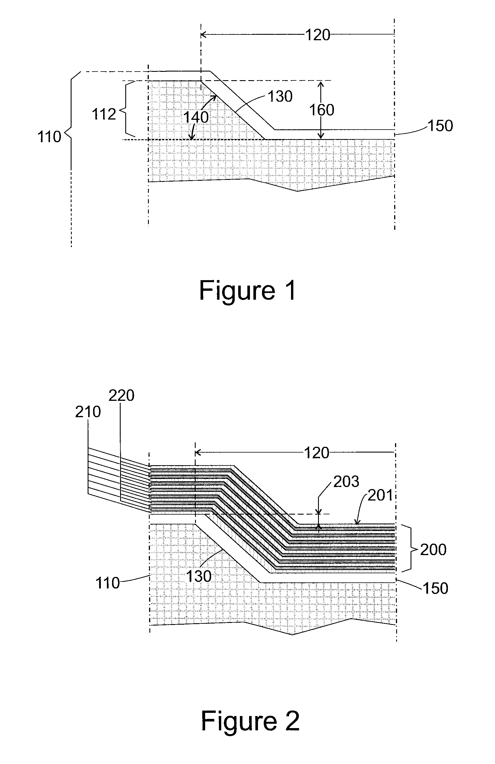
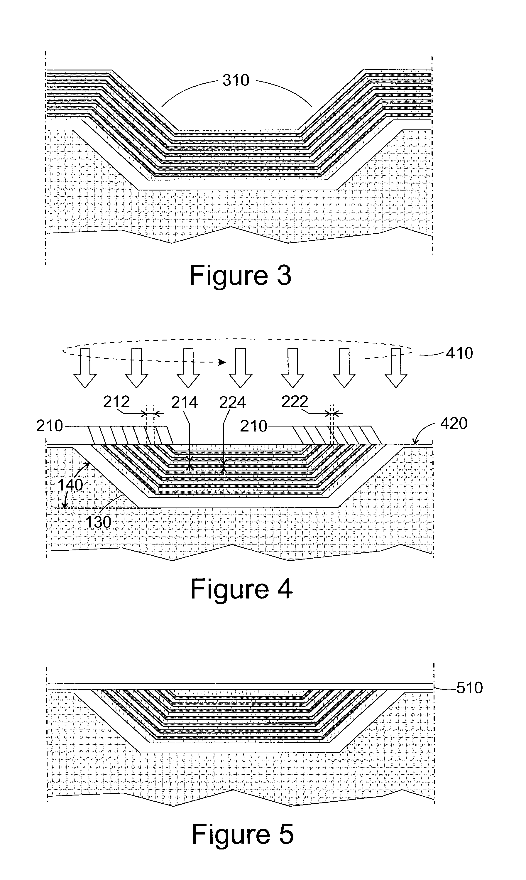
[0030]Before beginning a detailed review of embodiments of the invention, purely optional features that can if necessary be used in association according to all combinations with each other or alternatively, are stated below:[0031]the face of the substrate being electrically conductive, the stack is formed on the substrate with successively at least one alternation of an insulating layer and an electrically conductive layer;[0032]the wall of the pattern is electrically insulating and the stack is formed on the substrate with successively at least one alternation of an electrically conductive layer, a dielectric layer and an electrically conductive layer;[0033]the inclined wall is a flat surface;[0034]the angle formed between the inclined wall and the plane of the face of the face of the substrate is selected between 30° and 90°;[0035]the inclined wall is formed so as to splay as far as the face of the substrate from the wall of the bottom;[0036]the step of forming an electrical conn...


PUM


Abstract

A method for producing a microelectronic device including a substrate and a stack having at least one electrically conductive layer and at least one dielectric layer. The method includes formation, from one face of the substrate, of at least one pattern that is in depression with respect to a plane of the face of the substrate, the wall of the pattern having a bottom part and a flank part, the flank part being situated between the bottom part and the face of the substrate, the flank part having at least one inclined wall as far as the face of the substrate. With formation of the stack, the layers of the stack helping at least partially fill in the pattern. The stack is thinned of the stack at least as far as the plane of the face of the substrate so as to completely expose the edge of said at least one electrically conductive layer flush in one plane, and at least one electrical connection member is formed on the substrate in contact with the edge of the at least one electrically conductive layer.

Description

FIELD OF THE INVENTION[0001]The present invention concerns in general the formation of electrical contact points on each of the conductive layers of stratified structures alternating insulating and conductive layers and more particularly the production of multilayer capacitors or dense routing structures.PRIOR ART[0002]The microelectronics industry normally uses stratified structures of the metal / insulator / metal (MIM) type where layers, alternately insulating and conducting, are stacked in particular to form high-value capacitors at reasonable cost because of the economy of surface area that the superimposition of these layers affords.[0003]Structures of this type have already been described, in particular those based on the use of thin layers of ceramics separated by conductive sheets to produce high-value capacitors. For the lateral contact point, in order to connect all the conductive electrodes so as to put the individual capacitors in parallel, it is necessary to have recourse ...

Claims


Application Information

Patent Timeline
Patent Type & Authority Patents(United States)
IPC IPC(8): H05K3/02H05K13/04H01L49/02H01L23/522H05K3/10H01L27/02
CPCH05K13/046H01L23/5223H01L28/91H01L27/0203H01L2924/0002H01L2924/00
Inventor SIBUET, HENRI
Owner COMMISSARIAT A LENERGIE ATOMIQUE ET AUX ENERGIES ALTERNATIVES
Why Eureka
Try Eureka