Method for fabricating a plurality of opto-electronic semiconductor chips, and opto-electronic semiconductor chip

a technology of optoelectronic semiconductor chips and semiconductor chips, applied in the direction of semiconductor devices, basic electric elements, electrical apparatus, etc., can solve the problems of additional risk of failure, more difficult to obtain compact embodiments of led housings, etc., and achieve simple and cost-effective, good optoelectronic properties, and high efficiency

Active Publication Date: 2016-12-27
OSRAM OLED
View PDF16 Cites 4 Cited by
  • Summary
  • Abstract
  • Description
  • Claims
  • Application Information

AI Technical Summary

Benefits of technology

[0004]Embodiments of the invention provide a method for fabricating an optoelectronic semiconductor chip by which semiconductor chips distinguished by good optoelectronic properties can be fabricated in a simple and cost-effective manner. Furthermore, embodiments of the intention specify an optoelectronic semiconductor chip which is distinguished by a high efficiency and at the same time allows a compact configuration of the housing.
[0013]In a further preferred configuration, the carrier is thinned. This is preferably carried out after the semiconductor layer sequence has been fixed to the carrier and furthermore preferably before the recesses are formed. The required etching depth can be reduced as a result. The thinning is preferably carried out mechanically, for example, by grinding. Alternatively, however, a chemical method can also be employed.
[0022]Preferably, a mirror layer is applied to the semiconductor layer sequence before the semiconductor layer sequence is fixed to the carrier. The recesses extend through the mirror layer. During the operation of the semiconductor chips, radiation generated in the active region or radiation to be detected by the active region can be reflected at the mirror layer. The risk of absorption of radiation by the carrier is reduced as a result. The carrier can therefore also be radiation-nontransmissive to radiation generated in the active region or radiation to be detected by the active region. The mirror layer preferably contains a metal or a metallic alloy comprising at least one of the metals mentioned. In particular, silver or a silver-containing alloy is suitable for the visible spectral range. Furthermore, for the visible, in particular red, to infrared spectral range, the mirror layer can contain zinc, for example, for instance in the form of a zinc-containing alloy.
[0025]The carrier preferably contains a semiconductor material, in particular silicon. Silicon is available with a large area and in a cost-effective manner and, moreover, is distinguished by good microstructurability. For an electrically conductive connection of the second contact to the second semiconductor layer, the carrier is expediently doped.
[0029]In a preferred configuration, a mirror layer is arranged between the carrier and the semiconductor body. This reduces the risk of absorption of radiation in the carrier.

Problems solved by technology

However, such a wire bonding connection makes it more difficult to obtain compact embodiments of the LED housing and, moreover, constitutes an additional risk of failure.

Method used


Image

  • Method for fabricating a plurality of opto-electronic semiconductor chips, and opto-electronic semiconductor chip
  • Method for fabricating a plurality of opto-electronic semiconductor chips, and opto-electronic semiconductor chip
  • Method for fabricating a plurality of opto-electronic semiconductor chips, and opto-electronic semiconductor chip

Examples


Embodiment Construction

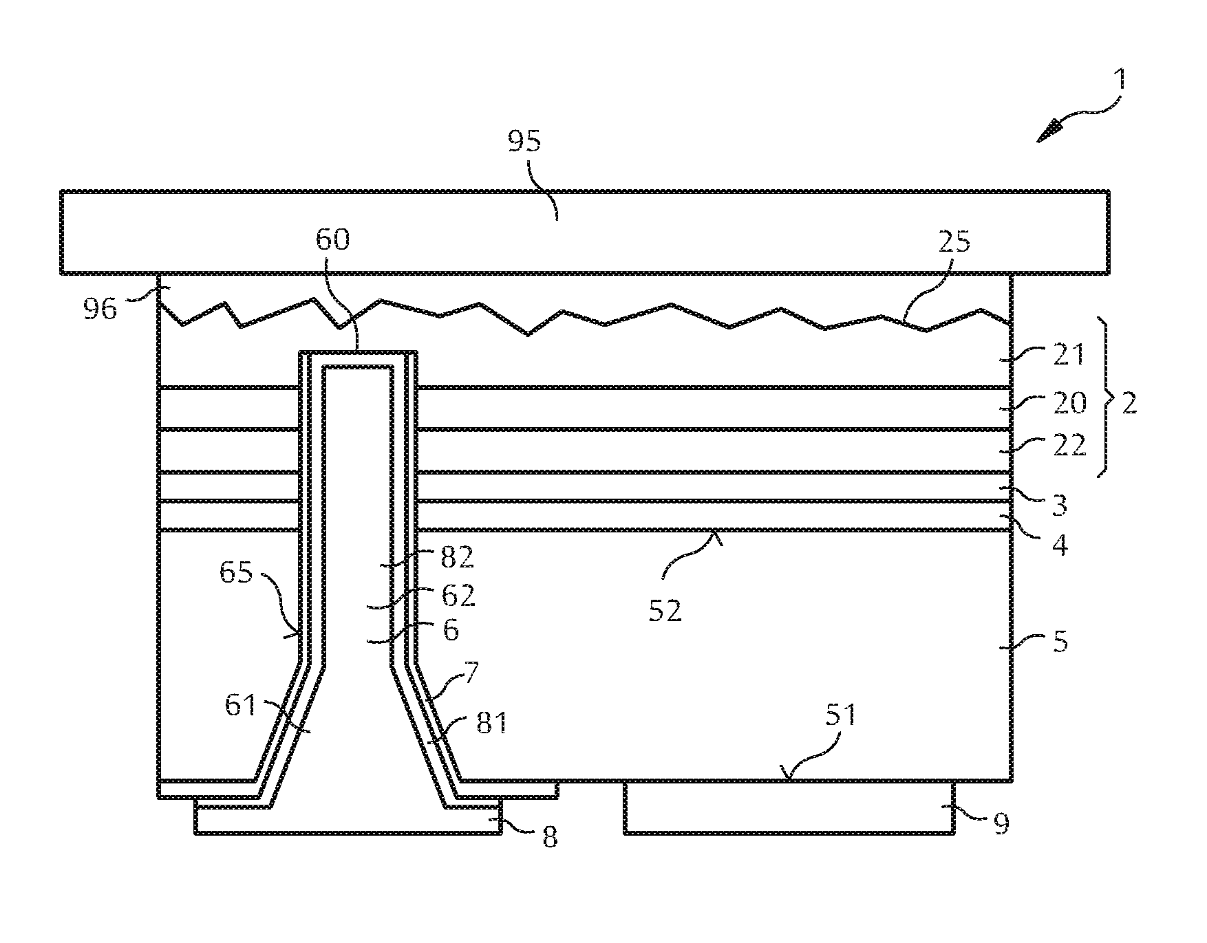
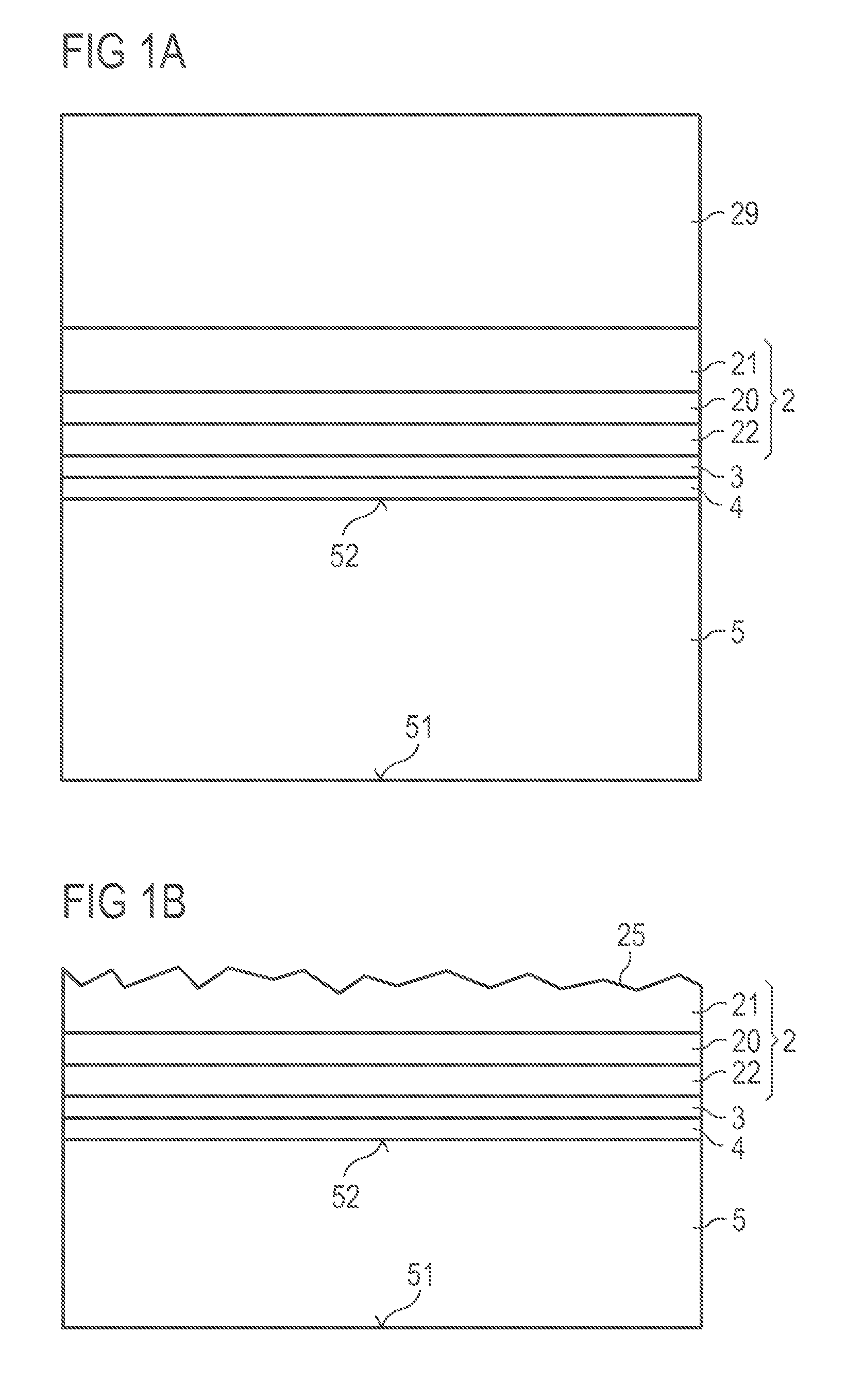
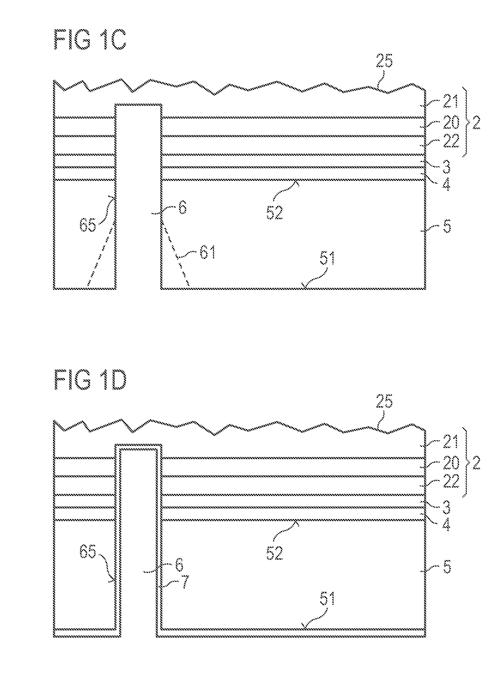
[0036]A first exemplary embodiment of a method for fabricating optoelectronic semiconductor chips is illustrated schematically with reference to FIGS. 1A to 1H. As shown in FIG. 1A, a semiconductor layer sequence is deposited preferably epitaxially, for example, by MOCVD, on a growth substrate 29. The semiconductor layer sequence has a first semiconductor layer 21 facing the growth substrate, an active region 20 and a second semiconductor layer 22 on a side of the active region that faces the first semiconductor layer 21. The first semiconductor layer and the second semiconductor layer differ from one another with regard to their conduction type. By way of example, the first semiconductor layer can be embodied as n-conducting and the second semiconductor layer as p-conducting, or vice versa. The first semiconductor layer and the second semiconductor layer can each comprise a plurality of partial layers.

[0037]For the sake of simplified illustration, the figures merely show an excerpt...


PUM


Abstract

A method for fabricating optoelectronic semiconductor chips and optoelectronic semiconductor chips are disclosed. In embodiments the method comprises depositing a semiconductor layer sequence having an active, the active region being arranged between a first semiconductor layer and a second semiconductor layer on a growth substrate, attaching the semiconductor layer sequence to a carrier and forming a plurality of recesses extending through the carrier, the second semiconductor layer and the active region into the first semiconductor layer. The method further comprises forming first contacts on a first main surface of the carrier, the first main surface facing away from the semiconductor layer sequence, wherein the first contacts are electrically conductively connected to the first semiconductor layer in the region of the recesses and singulating the carrier and the semiconductor layer sequence into the plurality of optoelectronic semiconductor chips, wherein each semiconductor chip has at least one recess.

Description

[0001]This patent application is a national phase filing under section 371 of PCT / EP2013 / 065187, filed Jul. 18, 2013, which claims the priority of German patent application 10 2012 106 953.0, filed Jul. 30, 2012, each of which is incorporated herein by reference in its entirety.TECHNICAL FIELD[0002]The present application relates to a method for fabricating optoelectronic semiconductor chips, and to an optoelectronic semiconductor chip.BACKGROUND[0003]Light-emitting diode semiconductor chips often have an electrical connection for the purpose of making electrical contact on the front side, the electrical contact being made with said electrical connection via a wire bonding connection. However, such a wire bonding connection makes it more difficult to obtain compact embodiments of the LED housing and, moreover, constitutes an additional risk of failure.SUMMARY OF THE INVENTION[0004]Embodiments of the invention provide a method for fabricating an optoelectronic semiconductor chip by w...

Claims


Application Information

Patent Timeline
Patent Type & Authority Patents(United States)
IPC IPC(8): H01L33/60H01L33/38H01L33/00H01L33/20H01L33/40
CPCH01L33/382H01L33/0079H01L33/20H01L33/60H01L33/405H01L2924/0002H01L2933/0016H01L2933/0025H01L2933/0033H01L2924/00H01L33/0093
Inventor NEUMANN, WOLFGANG
Owner OSRAM OLED
Why Eureka
Try Eureka