
Non-volatile memory cell and non-volatile memory device

a non-volatile memory and memory device technology, applied in the field of memory structure, can solve the problems of data loss, slow read/write speed, and inability to overwrite, and achieve the effects of fast reading speed, low power consumption, and simple structur

Active Publication Date: 2017-01-10
ALTO MEMORY TECH CORP +1
View PDF10 Cites 0 Cited by
  • Summary
  • Abstract
  • Description
  • Claims
  • Application Information

AI Technical Summary

Benefits of technology

The solution provides a memory cell with enhanced data stability and faster read / write speeds, addressing the limitations of conventional SRAM while maintaining low power consumption and data retention when powered off.

Problems solved by technology

In general, these two types of non-volatile memory are relatively stable and have less power consumption when storing data, but they are not easy to overwrite and have slower read / write speeds.
In practical, the capacitor of DRAM is periodically charged, and thus it has a disadvantage of higher power consumption.
When powered off, the data stored in a conventional SRAM is lost.
The conventional SRAM composed of six transistors still has some issues.
For example, when a static noise margin (SNM) of the memory cell is not enough, a storage node is vulnerable to the noise from an external bit line, and thus the original stored data is damaged when it is read.
Along with the trend of thin and light for mobile devices, the space for the electrical device is extremely limited, and the issue of the power consumption gets people's attentions even more.

Method used


Image

  • Non-volatile memory cell and non-volatile memory device
  • Non-volatile memory cell and non-volatile memory device
  • Non-volatile memory cell and non-volatile memory device

Examples


Embodiment Construction

[0024]Specific embodiments of the present invention are further described in detail below with reference to the accompanying drawings, however, the embodiments described are not intended to limit the present invention and it is not intended for the description of operation to limit the order of implementation. Moreover, any device with equivalent functions that is produced from a structure formed by a recombination of elements shall fall within the scope of the present invention. Additionally, the drawings are only illustrative and are not drawn to actual size. In accordance with the standard practice in the industry, various features are not drawn to scale. In fact, the dimensions of the various features may be arbitrarily increased or reduced for clarity of discussion.

[0025]Moreover, terms of “comprise”, “include”, “have”, etc. are open transitional phrases meaning “include but not limited to”. In addition, the usage “and / or” in the specification includes any one of the listed ite...


PUM


Abstract

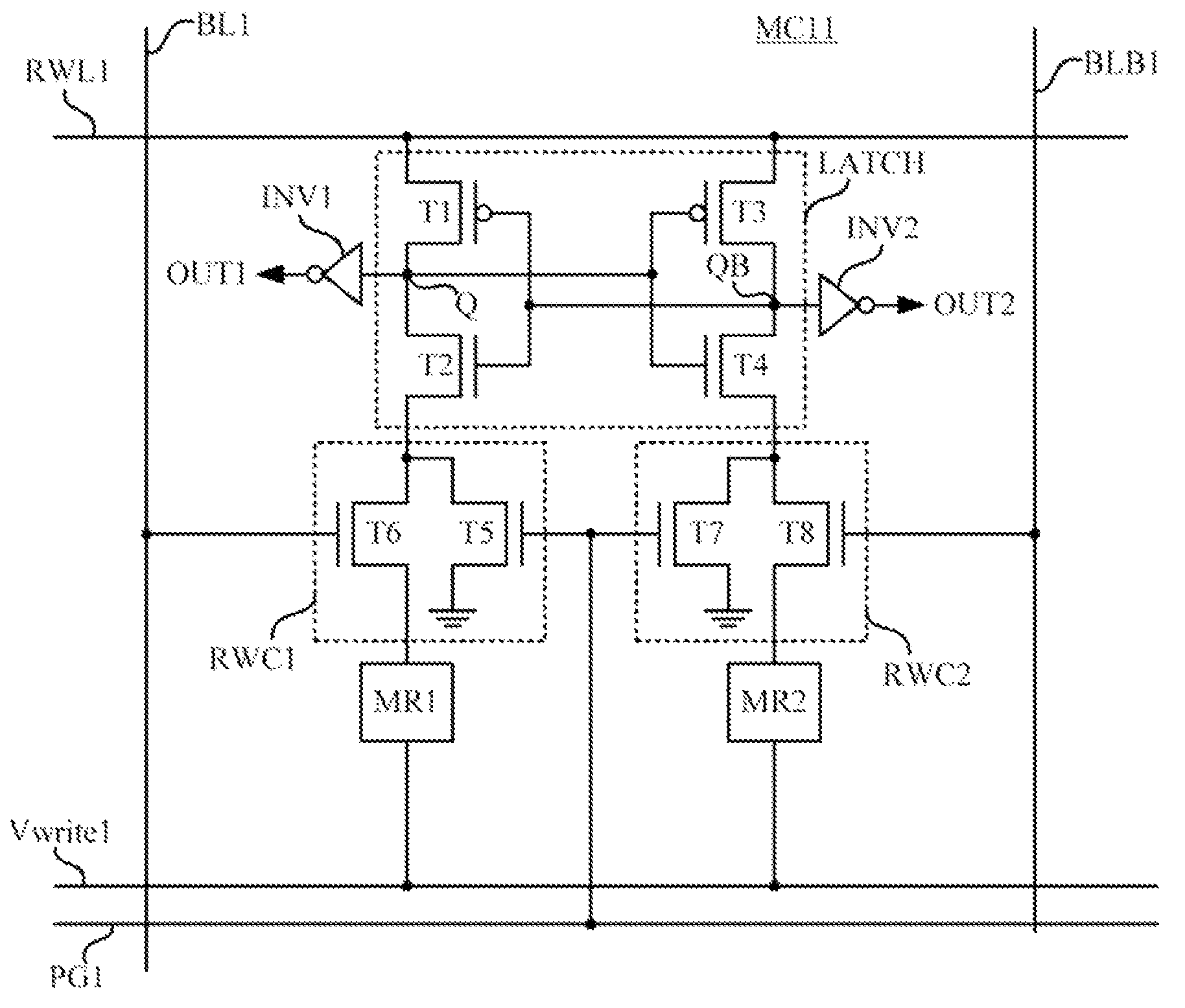
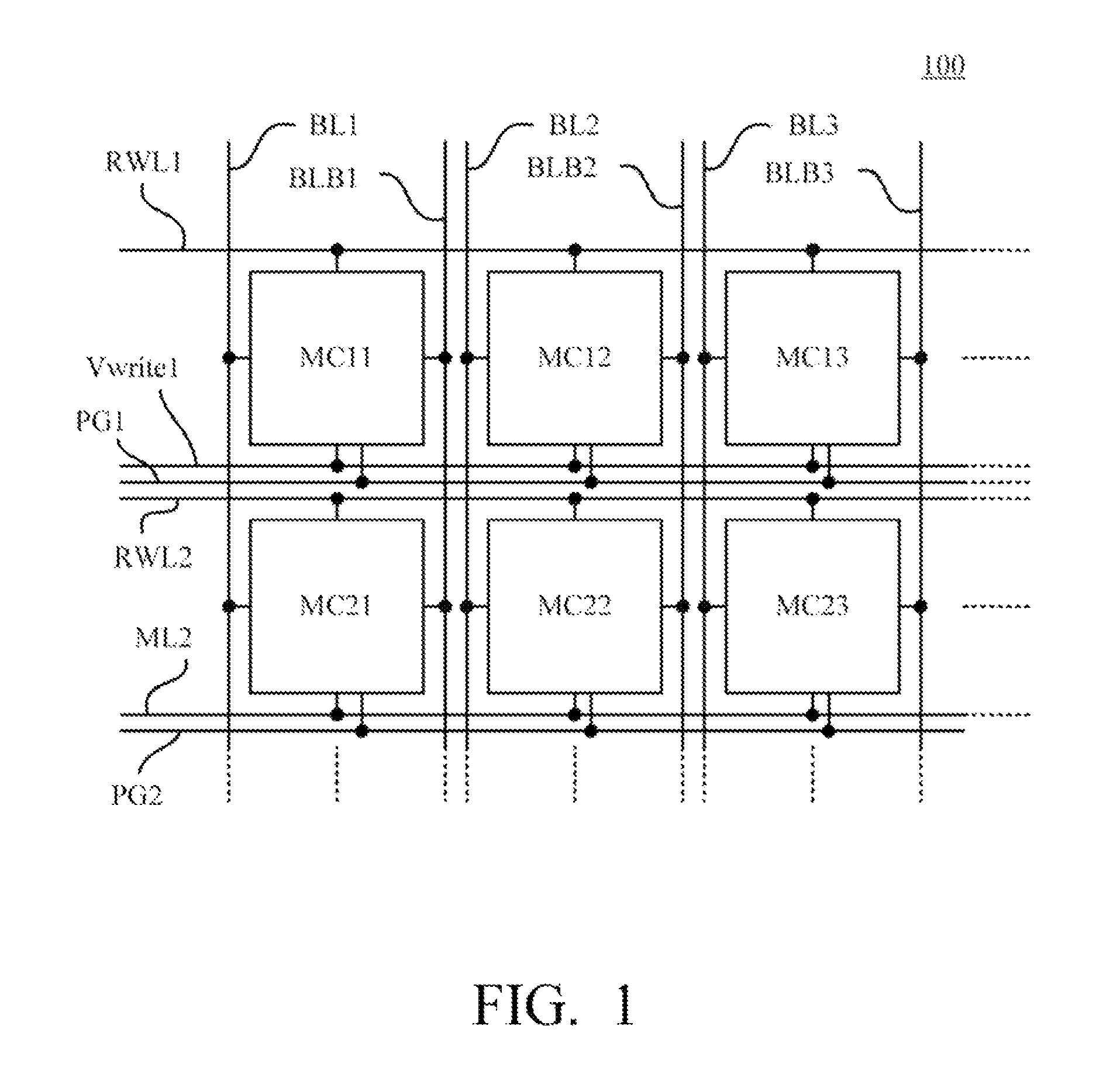
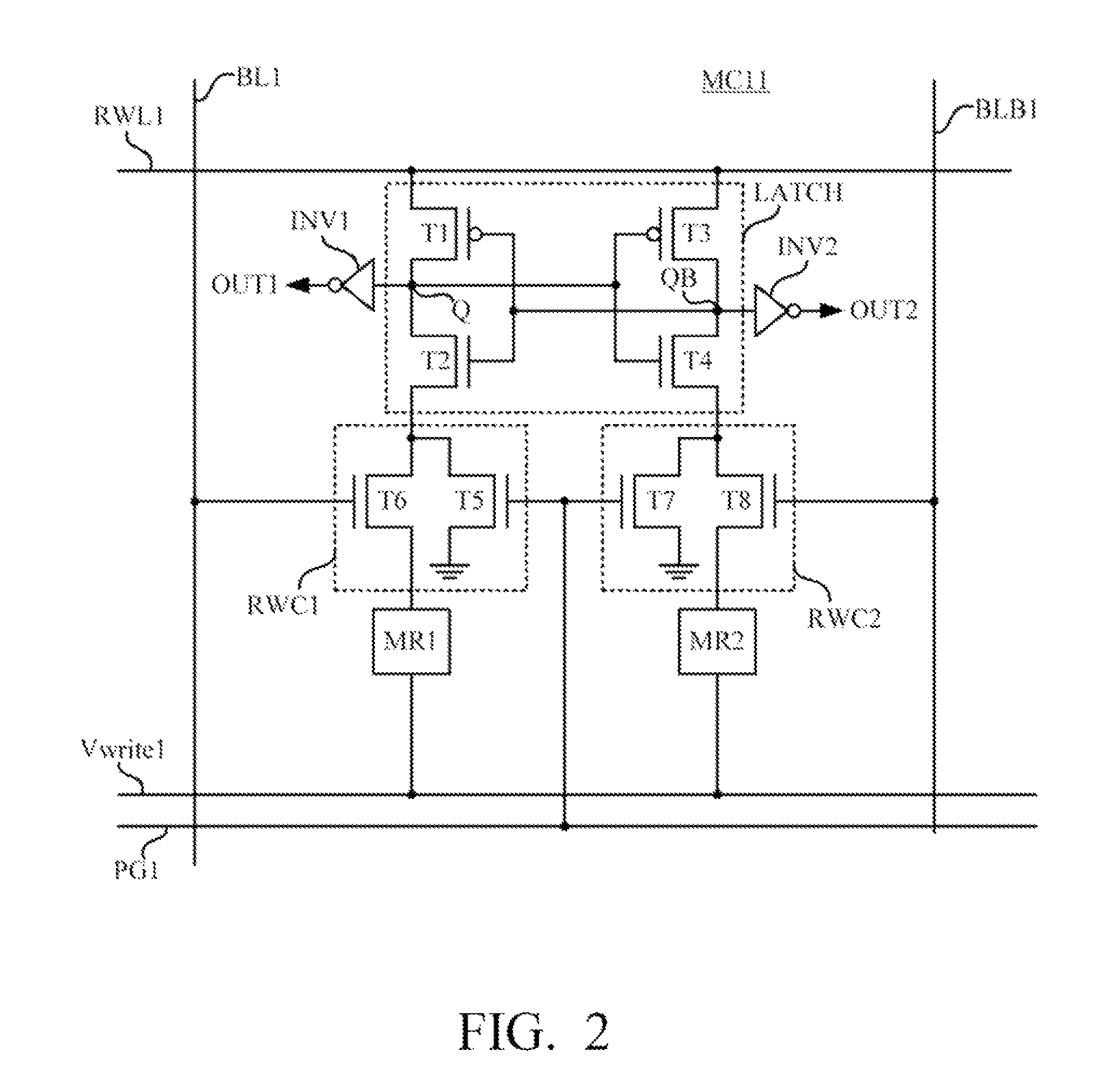
A non-volatile memory cell and a non-volatile memory device are provided. The non-volatile memory cell includes a latch structure, a first read / write circuit, a first memristor, a second read / write circuit and a second memristor. The first read / write circuit controls a writing operation of the first memristor. The second read / write circuit controls a writing operation of the second memristor. When a restore operation is performed, the data in the latch structure is restored by using the resistance difference between the first memristor and the second memristor. The non-volatile device of the invention combines the advantages of fast memory unit and non-volatile memory, and it may work at a high speed and retain data when powered off.

Description

RELATED APPLICATIONS[0001]This application claims priority to Chinese Application Serial Number 201510270878.1 filed on May 25, 2015, which is herein incorporated by reference.BACKGROUND[0002]Field of Invention[0003]The present invention relates to a memory structure. More particularly, the present invention relates to a non-volatile memory structure and related circuits.[0004]Description of Related Art[0005]Memory is an important component in a computer, and many different memory structures have been developed for different applications. For example, the memory structures include dynamic random access memory (DRAM), static random-access memory (SRAM), read-only memory (ROM), flash memory, etc.[0006]Among the memory structures, the ROM and the flash memory belong to non-volatile memory which can retain data when powered off. In general, these two types of non-volatile memory are relatively stable and have less power consumption when storing data, but they are not easy to overwrite a...

Claims


Application Information

Patent Timeline
Patent Type & Authority Patents(United States)
IPC IPC(8): G11C13/00
CPCG11C13/004G11C13/0004G11C13/0069G11C14/009G11C2013/009
Inventor WU, JUI-JENCHANG, JIA-HWANGHUANG, SHENG-TSAIJIEN, FAN-YI
Owner ALTO MEMORY TECH CORP
Learn More