Unlock instant, AI-driven research and patent intelligence for your innovation.

Substrate processing method

a processing method and substrate technology, applied in the direction of semiconductor devices, electrical equipment, electric discharge tubes, etc., can solve problems such as device performance degradation

Active Publication Date: 2017-01-31
TOKYO ELECTRON LTD
View PDF10 Cites 0 Cited by
  • Summary
  • Abstract
  • Description
  • Claims
  • Application Information

AI Technical Summary

Benefits of technology

The patent text describes a method for protecting a substrate from oxidation during processing. The method involves replacing the substrate's oxidized layer with a fluorine-based layer, which is exposed to an oxidizing atmosphere to protect the substrate. The fluorine-based layer is then removed using a plasma process, allowing for a clean substrate. The method can be used for various substrates and materials, such as Ge-containing substrates. The technical effect of the invention is to provide a suitable method for protecting substrates from oxidation during processing, which can improve the overall quality and efficiency of the process.

Problems solved by technology

One of the major issues with the high mobility channel such as Ge and III-V compound is the poor oxide and interface quality resulting in device performance degradation.

Method used


Image

  • Substrate processing method
  • Substrate processing method
  • Substrate processing method

Examples


Embodiment Construction

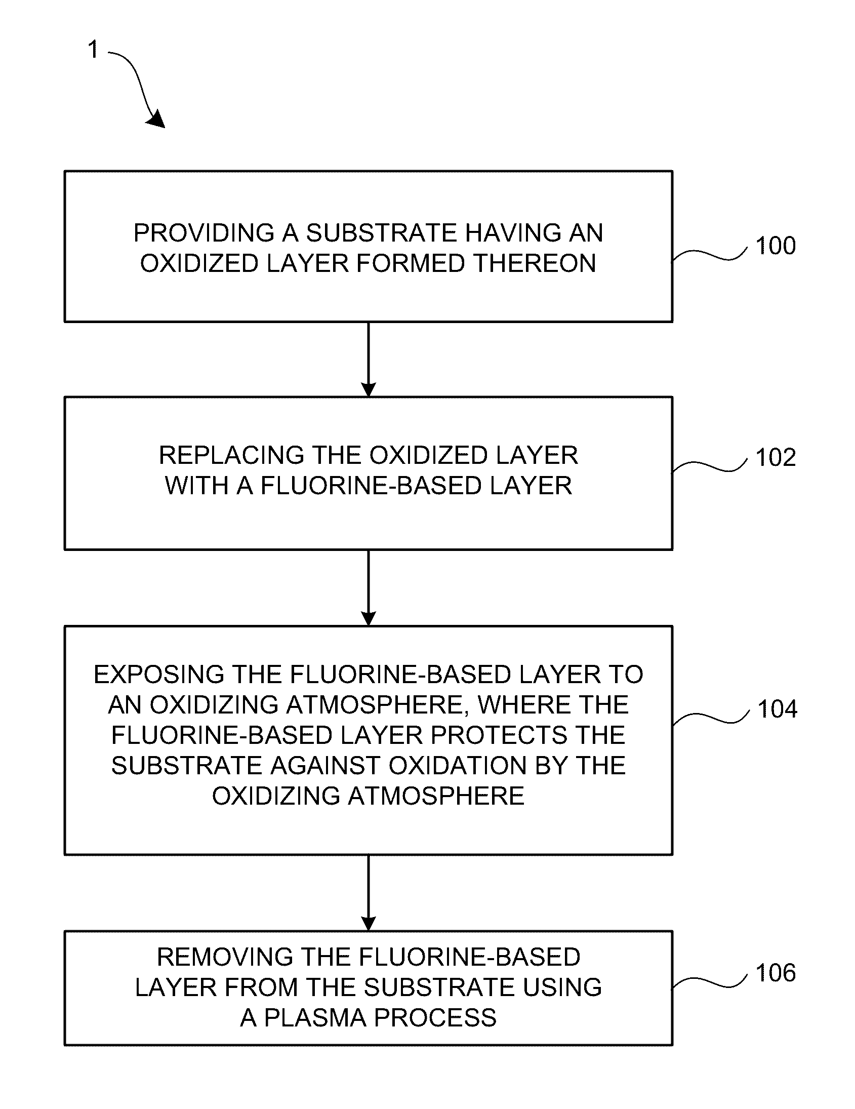
[0020]Embodiments of the invention provide a method for passivating a surface of a semiconductor substrate with fluorine-based layer in order to protect the surface against oxidation and allow longer queue times. The waiting time between processes for forming a semiconductor device are generally referred to as a queue time. A dry surface cleaning process is used to passivate the surface of the semiconductor substrate with the fluorine-based layer. The fluorine-based layer may be removed by a plasma process to provide a clean surface for further processing of the substrate. The method allows for improving semiconductor device performance such as interface trap density (Dit), mobility, and subthreshold swing (SS).

[0021]Embodiments of the invention are described below in reference to the Figures. According to one embodiment, a method is provided for processing a substrate. The method includes providing a substrate having an oxidized layer formed thereon, replacing the oxidized layer wi...


PUM


Abstract

A method for passivating a surface of a semiconductor substrate with fluorine-based layer to protect the surface against oxidation and allow longer queue times. According to one embodiment, the method includes providing a substrate having an oxidized layer formed thereon, replacing the oxidized layer with a fluorine-based layer, exposing the fluorine-based layer to an oxidizing atmosphere, where the fluorine-based layer protects the substrate against oxidation by the oxidizing atmosphere, and removing the fluorine-based layer from the substrate using a plasma process. According to another embodiment, the method includes providing a passivated substrate in a vacuum processing tool, the passivated substrate having a fluorine-based layer thereon that is effective for protecting the passivated substrate against oxidation by an oxidizing atmosphere, removing the fluorine-based layer from the passivated substrate using a microwave plasma process in the vacuum processing tool, thereby forming a clean substrate, and processing the clean substrate under vacuum conditions.

Description

[0001]This application claims priority to U.S. Provisional Patent Application No. 62 / 036,474 filed on Aug. 12, 2014, the contents of which is incorporated herein by reference in its entirety.FIELD OF THE INVENTION[0002]The present invention generally relates to processing of a substrate in semiconductor manufacturing, and more particularly to a method of passivating a surface of a semiconductor substrate with fluorine-based layer in order to protect the surface against oxidation and allow longer queue times.BACKGROUND OF THE INVENTION[0003]Devices with a high-mobility channel, such as, SiGe, Ge and III-V semiconductors offer the possibility of increased device performance beyond traditional Si-based devices. In particular, Ge is an attractive candidate due to its lower effective mass and higher mobility for charge carriers compared to Si. One of the major issues with the high mobility channel such as Ge and III-V compound is the poor oxide and interface quality resulting in device p...

Claims


Application Information

Patent Timeline
Patent Type & Authority Patents(United States)
IPC IPC(8): H01L21/311H01L21/02H01L29/16H01L21/28H01L29/161H01L29/51
CPCH01L21/31116H01L21/0206H01L21/02252H01L21/02337H01L21/28238H01L21/28255H01L29/16H01L29/161H01L29/513H01L29/517H01L21/306H01L21/3105H01L21/31122H01L21/321H01J37/32192
Inventor TAPILY, KANDABARA N.AMANO, FUMITAKA
Owner TOKYO ELECTRON LTD