
Layer system, energy store, and method for manufacturing an energy store
a technology of energy storage and layer system, which is applied in the direction of cell components, final product manufacturing, sustainable manufacturing/processing, etc., can solve the problems of limited power level and associated environmental problems of electrolytes, and achieve the effects of improving stability of layer system, low stability, and reducing the height of layer system according to the present invention
- Summary
- Abstract
- Description
- Claims
- Application Information
AI Technical Summary
Benefits of technology
Problems solved by technology
Method used
Image

Examples
Embodiment Construction
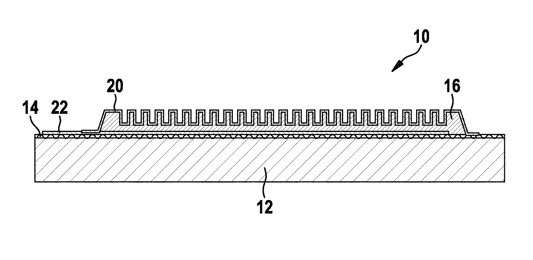
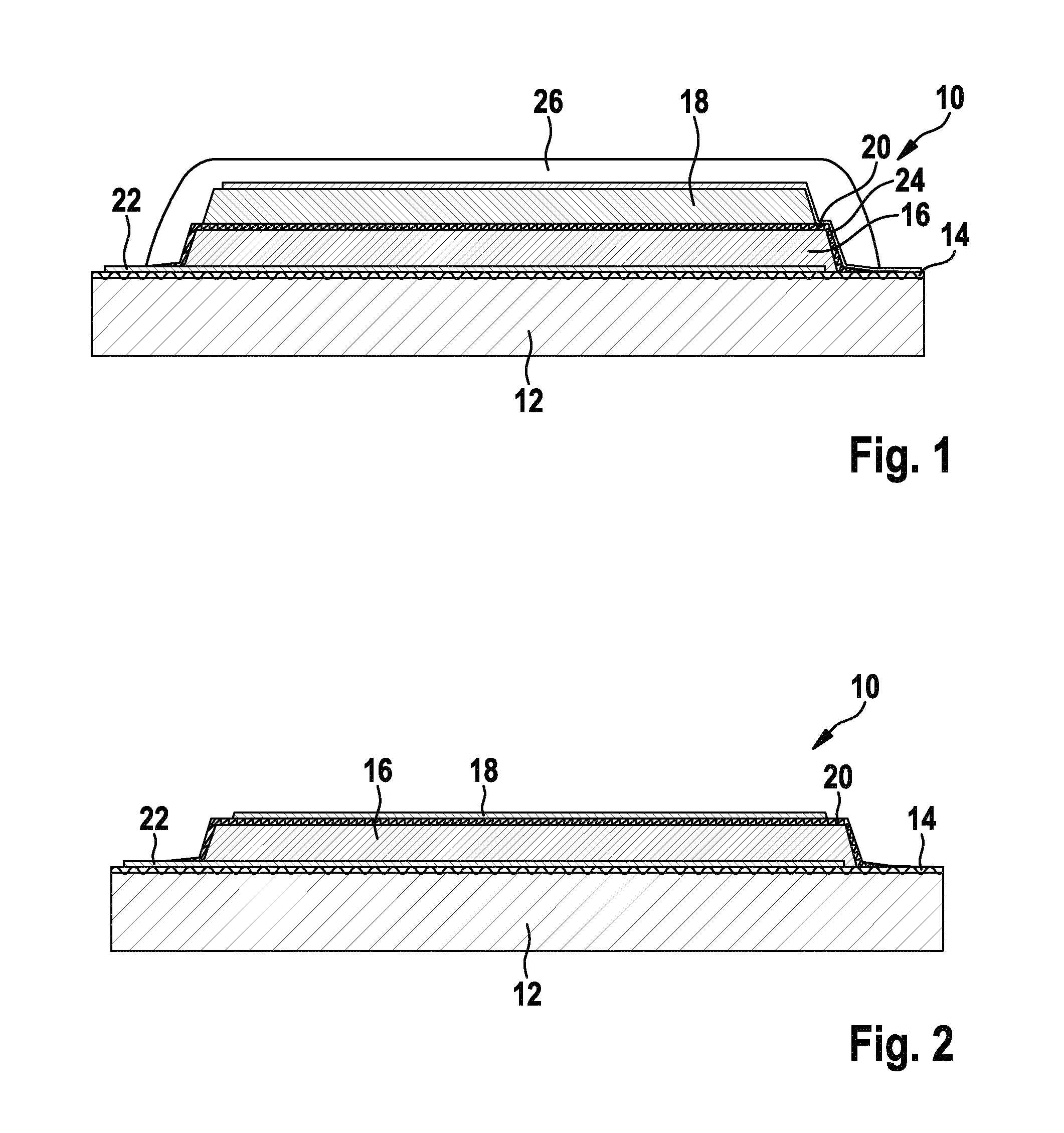
[0051]FIG. 1 shows one exemplary embodiment of layer system 10 according to the present invention. Layer system 10 may, for example, be part of an energy store, a lithium-ion accumulator, for example, or may form same.
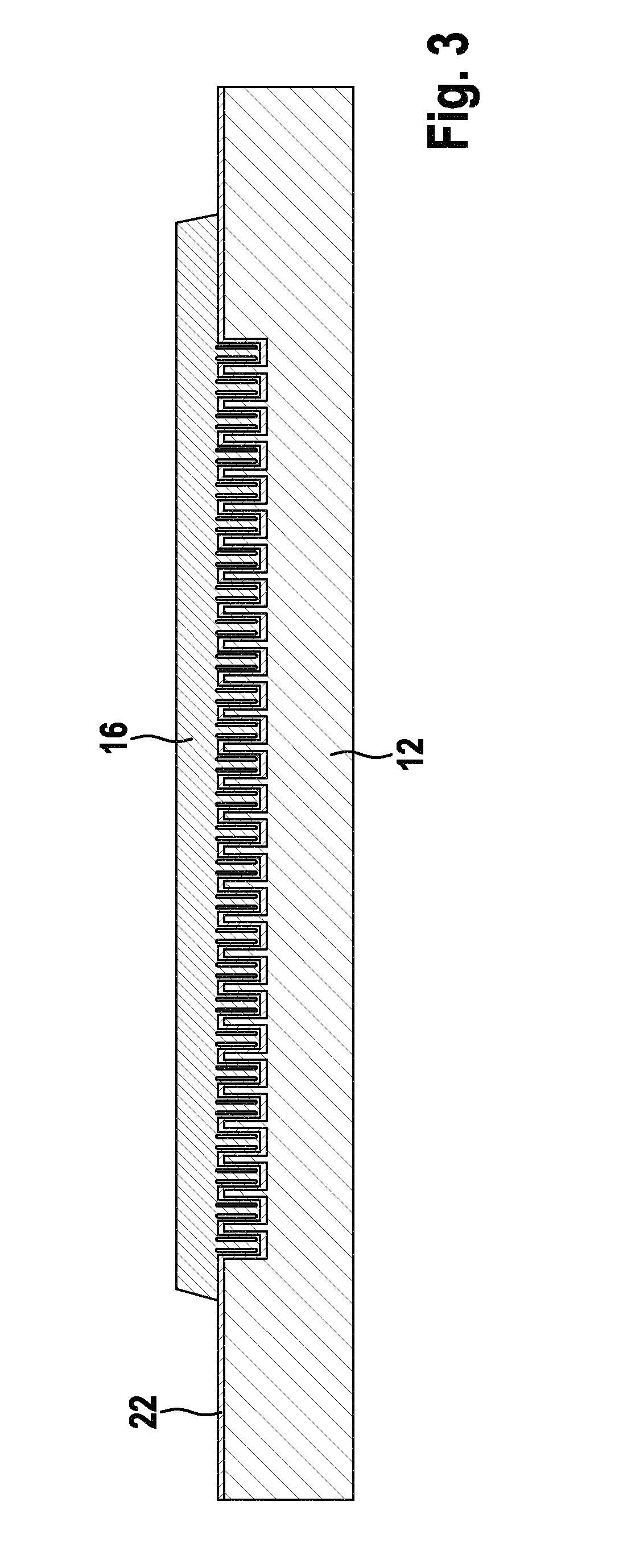
[0052]Layer system 10 according to the present invention may include a substrate 12 as a carrier. For this purpose, substrate 12 may be used to impart more stability to the layers. However, substrate 12 is only optional and does not necessarily have to be present. For example, substrate 12 may be dispensed with if the layers have sufficient stability. Substrate 12 is formed, for example, from a semiconductor material or MEMS material such as silicon or glass. In addition, substrate 12 may be made of a polymer or a metal. It is advantageous for the surface of substrate 12 to be electrically insulating. For this purpose, an insulating layer 14 may be provided on substrate 12 if the material of the substrate is not electrically insulating per se. For example, this insulat...
PUM
| Property | Measurement | Unit |
|---|---|---|
| thicknesses | aaaaa | aaaaa |
| thicknesses | aaaaa | aaaaa |
| electrical conductivity | aaaaa | aaaaa |
Abstract
Description
Claims
Application Information