
Current switching transistor

a current switching transistor and transistor technology, applied in the field of transistors, can solve the problems of depletion or enhancement of the number, the inability to modulate the source-drain current, and the inability to meet the requirements of the application, and the progress in developing the application of transistors to some extent is hindered by the complexity of the printed transistor

Inactive Publication Date: 2017-03-21
PST SENSORS
View PDF24 Cites 4 Cited by
  • Summary
  • Abstract
  • Description
  • Claims
  • Application Information

AI Technical Summary

Benefits of technology

The patent describes how to change the resistance of certain components called varistors by adjusting their size and number of semiconductor bridges. This allows for greater flexibility in the component's performance while maintaining its easy access to three terminals.

Problems solved by technology

In field effect transistors the main cause of the modulation of the source-drain current is the depletion or enhancement of the number of free charge carriers in the semiconductor material by the electric field resulting from the application of a potential to the gate.
Progress in developing these applications has to some extent been hindered by the complexity of the printed transistor, which requires exact control of the properties, compatibility during processing, arrangement and thickness of multiple layers of different materials.

Method used


Image

  • Current switching transistor
  • Current switching transistor
  • Current switching transistor

Examples


examples

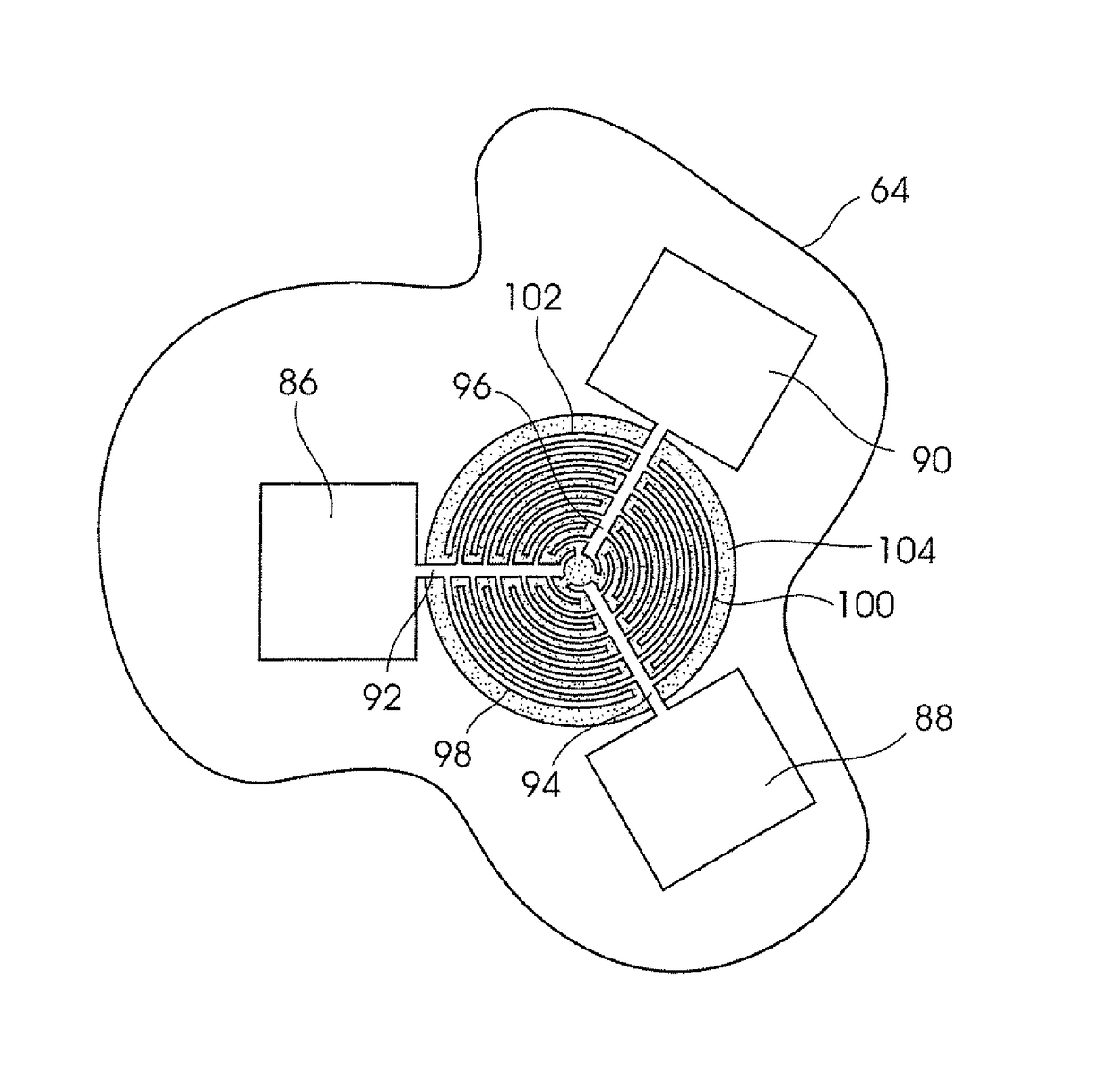
[0093]FIG. 9 shows a photograph of a prototype transistor of the third embodiment (FIG. 6) which has been produced by screen printing of conducting and semiconducting inks. The substrate comprises uncoated wood-free paper of weight 80 gram per square metre. Other examples of this embodiment were also fabricated on 160 gsm uncoated paper board and on 100 micron PET.

[0094]The contacts and other conducting parts of the device are printed using Du Pont Luxprint 5000 silver conductor. Similar devices have been produced in which the contacts have been printed with silver and silver alloy inks sourced from other manufacturers, including Creative Materials Inc. and PChem Inc.; and also using Du Pont 7162 Luxprint translucent conductor, which provides a semiconducting material with a constant electric field-independent resistivity.

[0095]The semiconducting pattern was printed using an ink comprising silicon nanoparticles and an acrylic binder. The silicon nanoparticles employed were of the ty...


PUM


Abstract

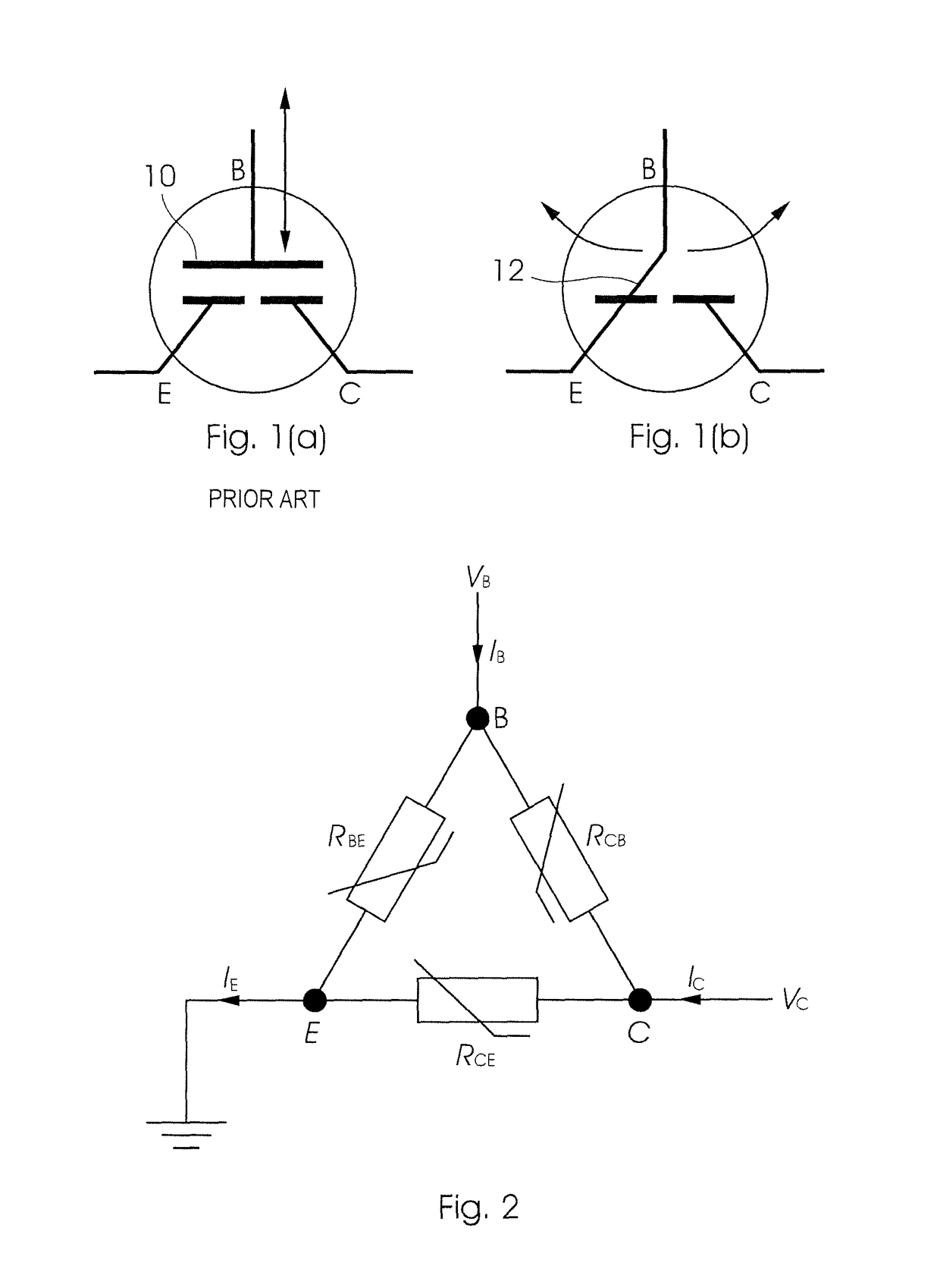
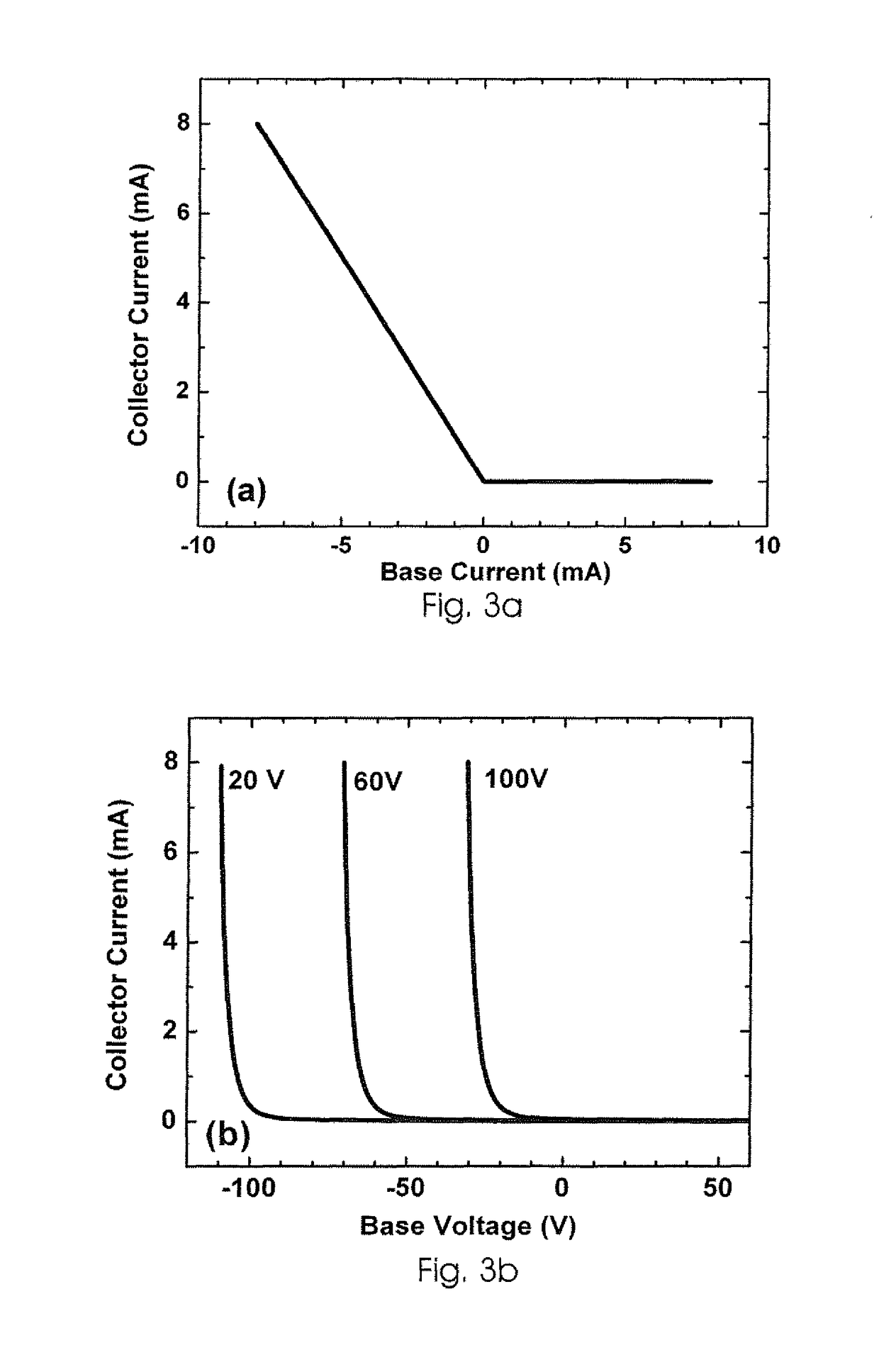
An electronic device and a method of fabricating an electronic device are disclosed. The device includes a body of semiconductor material, and a conductive material defining at least three conducting contacts to form respective terminals. The semiconductor material and the conducting contacts overlap at least partially to define the device, so that the electrical characteristics of the device between any pair of terminals correspond to those of a varistor. The body of semiconductor material may be a layer deposited by printing or coating. The varistor characteristics between each pair of terminals enable switching of an electrical current between one terminal and any two other terminals in such a manner that when there is a positive current into a first terminal, there is a negligible current through a second terminal at which a positive potential is applied and a positive current out of a third terminal which is held at a negative potential with respect to the second terminal. When there is a negative current outwards of the first terminal, there is a positive current into the second terminal and a negligible current through the third terminal.

Description

BACKGROUND OF THE INVENTION[0001]THIS invention relates to an electronic device, in particular a transistor, and to methods of fabricating such a device.[0002]This invention further relates to the field of printed electronics, which is the fabrication of electronic devices and circuitry using printing, coating and packaging techniques.[0003]Transistors, being electronic devices which exhibit a transconductance or transresistance, are well known in the art. Commonly transistors are divided into two classes: junction transistors and field effect transistors (FETs). The principle of operation of the FET and a design for a junction FET were first disclosed by Lilienfeld in CA 272,437 on 22 Oct. 1925, and a variation, of the insulated gate FET (IG-FET) by Bardeen in U.S. Pat. No. 2,524,033, filed on 26 Feb. 1948. The bipolar junction transistor (BJT) was first disclosed by Shockley on the same date in U.S. Pat. No. 2,569,347. Working with Brattain, Bardeen and Shockley developed the poin...

Claims


Application Information

Patent Timeline
Patent Type & Authority Patents(United States)
IPC IPC(8): H01L29/00H01L29/70H01L29/04H01L29/06H10N97/00
CPCH01L29/705H01L29/04H01L29/0692H01L29/72H10K85/1135H10K85/113H10K10/00H01C7/1013H10N99/00H10N97/00
Inventor BRITTON, DAVID THOMASHAERTING, MARGITWALTON, STANLEY DOUGLAS
Owner PST SENSORS
Learn More