Contact probe pin

a technology of contact probe and probe body, which is applied in the direction of coupling contact members, instruments, measurement devices, etc., can solve the problems of difficult contact, deterioration of contact pins, so as to achieve stable electrical contact and high temperature in the usage environment

Active Publication Date: 2017-04-18
KOBE STEEL LTD +1
View PDF34 Cites 4 Cited by
  • Summary
  • Abstract
  • Description
  • Claims
  • Application Information

AI Technical Summary

Benefits of technology

[0033]In the contact probe pin of the present invention, a carbon film containing a metal element is formed on a surface of a projection obtained by dividing a tip into two or more, and the radius of curvature at an apex part of the above-mentioned projection is adjusted to 30 μm or more. Accordingly, there can be realized the contact probe pin in which adherence of Sn and or like can be reduced as much as possible to be able to maintain stable electrical contact over a long period of time, even under such circumstances that the temperature of a usage environment is high.

Problems solved by technology

However, it is sometimes deteriorated to several hundred mΩ to several Ω by repeated tests on the test surfaces.
However, this sometimes significantly lowers reliability of a test process and an operating rate, so that other countermeasures have been studied.
In particular, a solder material, a Sn-plated electrode or the like has a property of being scraped off to easily adhere to surfaces of the contact terminals because of its softness, and a surface thereof is easily oxidized to cause high resistance, which makes it difficult to perform contact while maintaining a stable resistance value.
However, in the contact probe pin composed of this material, an electrode material (particularly, Sn) from a material such as a solder material or Sn plating easily adheres to the tip of the contact probe pin, and the adhered electrode material is surface-oxidized, which causes a problem that the contact resistance value of the contact probe pin becomes unstable.

Method used


Image

  • Contact probe pin
  • Contact probe pin
  • Contact probe pin

Examples


examples

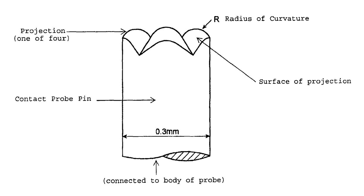
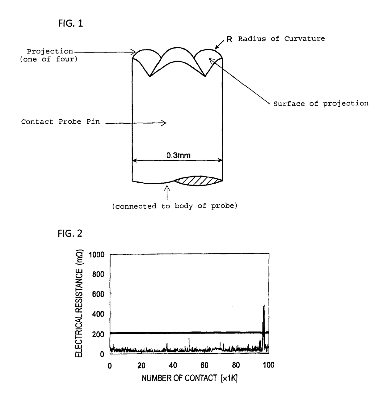
[0056]As a contact probe pin, a spring built-in probe with a tip divided into four projections and with apex parts of the projections having a radius of curvature of 50 μm (R=0.05 mm) was prepared, as shown in FIG. 1 (a schematic illustration showing an example of an appearance shape). The entire tip has a diameter of 0.3 mm (300 μm). A surface of this contact probe pin was Au-plated, and a base material was made of Be—Cu (a commercial product). FIG. 1 schematically shows a state in which the tip is projected from a side surface, and the shape thereof is illustrated as three projections. Further, when it is come into contact with an other electrode to be pressed through a predetermined stroke by a function of the spring, a load of 30 gf (147 N / mm2) is generated.

[0057]A carbon (graphite) target, a Cr target and a Ni target were each arranged in a magnetron sputtering apparatus, and the contact probe pin (base material) was arranged in a position opposed thereto. After the sputtering ...


PUM


Abstract

The present invention provides a contact probe pin in which a carbon film having both of conductivity and durability is formed on a base material with a tip divided, wherein Sn adherence can be reduced as much as possible to be able to maintain stable electrical contact over a long period of time, even under such circumstances that the temperature of a usage environment becomes high. The present invention relates to a contact probe pin, including a tip divided into 2 or more projections and repeatedly coming into contact with a test surface at the projection, wherein a carbon film containing a metal element is formed at least on a surface of the projection, and a radius of curvature at an apex part of the projection is 30 μm or more.

Description

TECHNICAL FIELD[0001]The present invention relates to a contact probe pin, which is used for testing electrical properties of semiconductor elements and includes a configuration in which a tip is divided into a plurality of projections, and particularly to a contact probe pin having such excellent durability that conductivity is not deteriorated by repeated tests.BACKGROUND ART[0002]Electrical properties of electronic parts such as an integrated circuit (IC), a large-scale integrated circuit (LSI) and a light-emitting diode (LED) (in other wards, electronic parts using semiconductor elements) are tested by bringing probe pins into contact with electrodes of the semiconductor elements. Such probe pins (contact probe pins) used in test devices (semiconductor test devices) are required not only to have good conductivity (a low contact resistance value), but also to show a stable resistance value (the contact resistance value is not fluctuated) even by repeated contact with surfaces (te...

Claims


Application Information

Patent Timeline
Patent Type & Authority Patents(United States)
IPC IPC(8): G01R1/067H01R13/03
CPCG01R1/06761G01R1/06738H01R13/03G01R1/067
Inventor HIRANO, TAKAYUKIKOBORI, TAKASHI
Owner KOBE STEEL LTD
Why Eureka
Try Eureka