Semiconductor device and related manufacturing method

a semiconductor device and manufacturing method technology, applied in the manufacture of electrode systems, electric discharge tubes/lamps, tubes with electrostatic control, etc., can solve the problems of insufficient control of electron transmission, insufficient and timely control of off of vft, and substantial energy consumption of vft operation, so as to achieve efficient energy utilization, effective control, and satisfactory controllability of semiconductor devices

Active Publication Date: 2017-07-25
SEMICON MFG INT (SHANGHAI) CORP
View PDF6 Cites 6 Cited by
  • Summary
  • Abstract
  • Description
  • Claims
  • Application Information

AI Technical Summary

Benefits of technology

[0027]According to embodiments of the present invention, an electric field between the source electrode and the drain electrode may be substantially surrounded and / or enclosed by the gate electrode. Therefore, the on and off of an electron flow between the source electrode and the drain electrode may be substantially effectively controlled, and energy may be efficiently utilized. Advantageously, controllability of the semiconductor device may be satisfactory, and energy consumption of the semiconductor device may be minimized.

Problems solved by technology

As a result, transmission of electrons may not be sufficiently controlled, such that the on and off of the VFT may not be effectively and timely controlled.
For achieving desirable control of the VFT, additional voltage may be required, such that the operation of the VFT may require substantially high energy consumption.

Method used


Image

  • Semiconductor device and related manufacturing method
  • Semiconductor device and related manufacturing method
  • Semiconductor device and related manufacturing method

Examples


Embodiment Construction

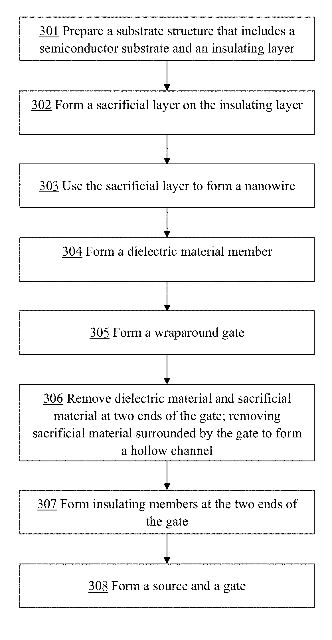
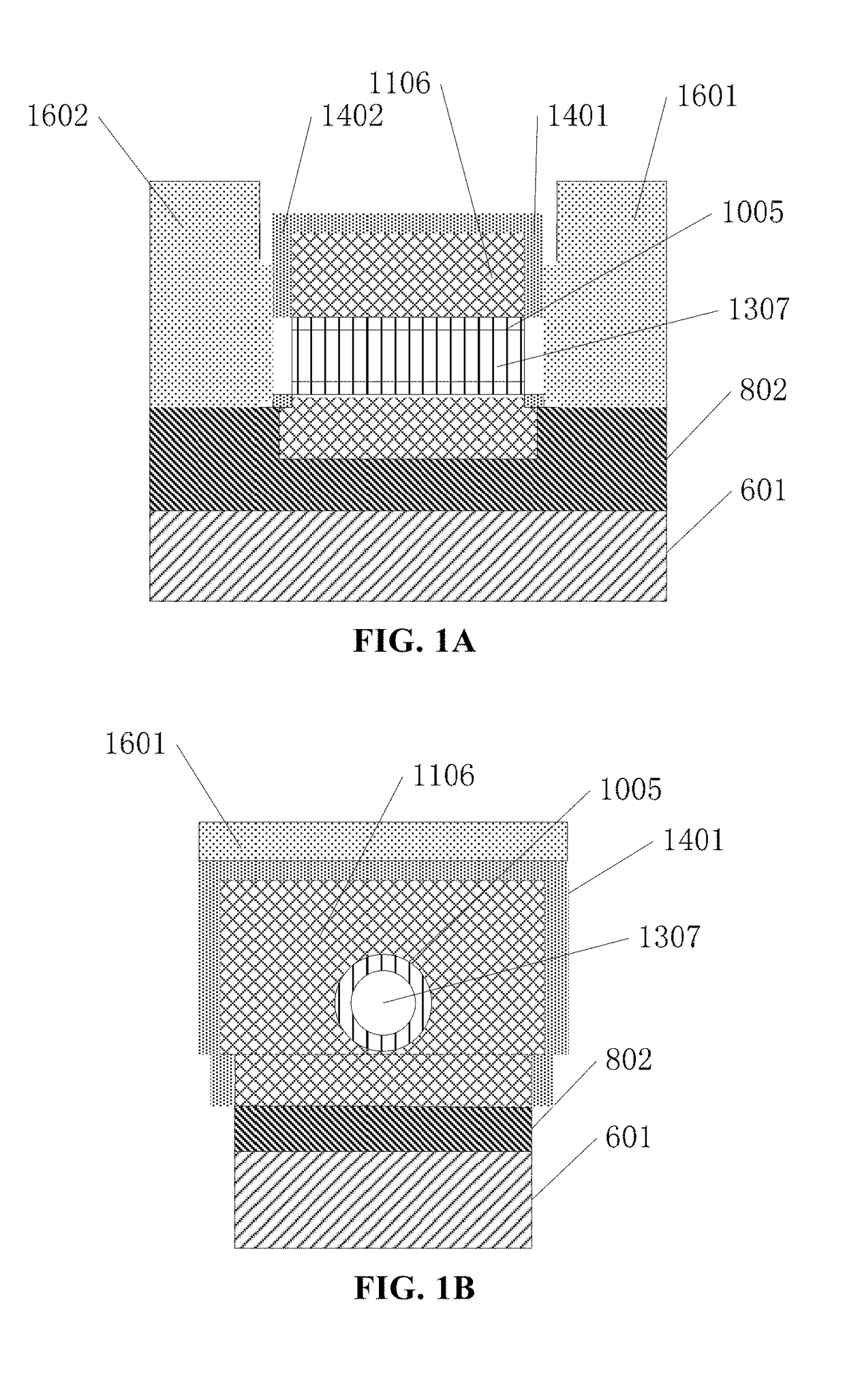
[0060]Example embodiments of the present invention are described with reference to the accompanying drawings. As those skilled in the art would realize, the described embodiments may be modified in various different ways, all without departing from the spirit or scope of the present invention. Embodiments of the present invention may be practiced without some or all of these specific details. Well known process steps and / or structures may not have been described in detail in order to not unnecessarily obscure the present invention.

[0061]The drawings and description are illustrative and not restrictive. Like reference numerals may designate like (e.g., analogous or identical) elements in the specification. Repetition of description may be avoided.

[0062]The relative sizes and thicknesses of elements shown in the drawings are for facilitate description and understanding, without limiting the present invention. In the drawings, the thicknesses of some layers, films, panels, regions, etc...


PUM


Abstract

A semiconductor device may include the following elements: a semiconductor substrate, an insulator positioned on the substrate, a source electrode positioned on the insulator, a drain electrode positioned on the insulator, a gate electrode positioned between the source electrode and the drain electrode, a hollow channel surrounded by the gate electrode and positioned between the source electrode and the drain electrode, a dielectric member positioned between the hollow channel and the gate electrode, a first insulating member positioned between the gate electrode and the source electrode, and a second insulating member positioned between the gate electrode and the drain electrode.

Description

CROSS-REFERENCE TO RELATED APPLICATION[0001]This application claims priority to and benefit of Chinese Patent Application No. 201410129139.6, filed on 1 Apr. 2014, the Chinese Patent Application being incorporated herein by reference in its entirety.BACKGROUND OF THE INVENTION[0002]The present invention is related to a semiconductor device and a method for manufacturing the semiconductor device.[0003]Semiconductor devices, such as vacuum field effect transistors (VFTs), may be used in place of vacuum tubes in various applications, such as one or more of stereo systems, microwave ovens, satellites, etc.[0004]As an example, a vacuum field effect transistor (VFT) may include a source electrode, a drain electrode, a vacuum channel positioned between the source and the drain electrode, a gate electrode positioned under the source electrode and the drain electrode, an insulator that insulates the gate electrode from the source electrode and the drain electrode, and a substrate for support...

Claims


Application Information

Patent Timeline
Patent Type & Authority Patents(United States)
IPC IPC(8): H01J19/38H01J9/14H01J21/06H01J9/385H01J9/24
CPCH01J21/06H01J9/148H01J9/24H01J9/385H01J19/38H01J19/28
Inventor XIAO, DEYUAN
Owner SEMICON MFG INT (SHANGHAI) CORP
Why Eureka
Try Eureka