
Piezoelectric thin film and method for producing the same

a thin film and piezoelectric technology, applied in the field of piezoelectric thin film, can solve the problem that the excellent piezoelectric properties of the piezoelectric thin film may not always be obtained, and achieve the effect of reducing the degree of deterioration of the piezoelectric properties and achieving the greater piezoelectric d33 coefficien

Active Publication Date: 2017-08-15
DENSO CORP +1
View PDF13 Cites 0 Cited by
  • Summary
  • Abstract
  • Description
  • Claims
  • Application Information

AI Technical Summary

Benefits of technology

The approach results in piezoelectric thin films with improved and consistent piezoelectric properties, comparable to those without carbon contamination, by effectively limiting the carbon atomic content, thereby enhancing the piezoelectric d33 coefficient.

Problems solved by technology

Thus, a piezoelectric thin film which exhibits excellent piezoelectric properties may not be always obtained.

Method used


Image

  • Piezoelectric thin film and method for producing the same
  • Piezoelectric thin film and method for producing the same
  • Piezoelectric thin film and method for producing the same

Examples


example 1

[0039]Next, an example and a comparative example of the piezoelectric thin film are explained.

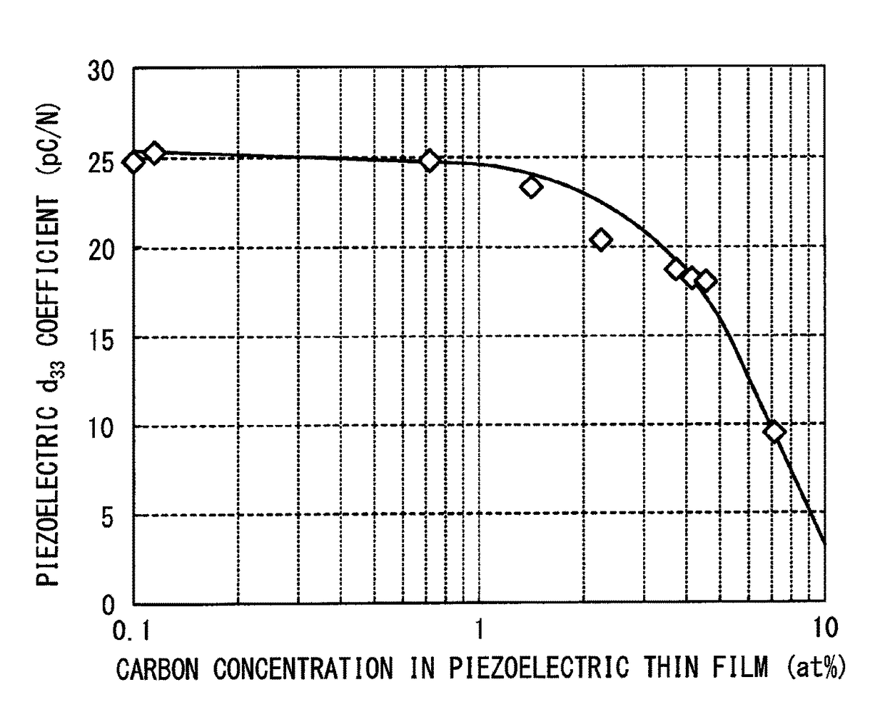
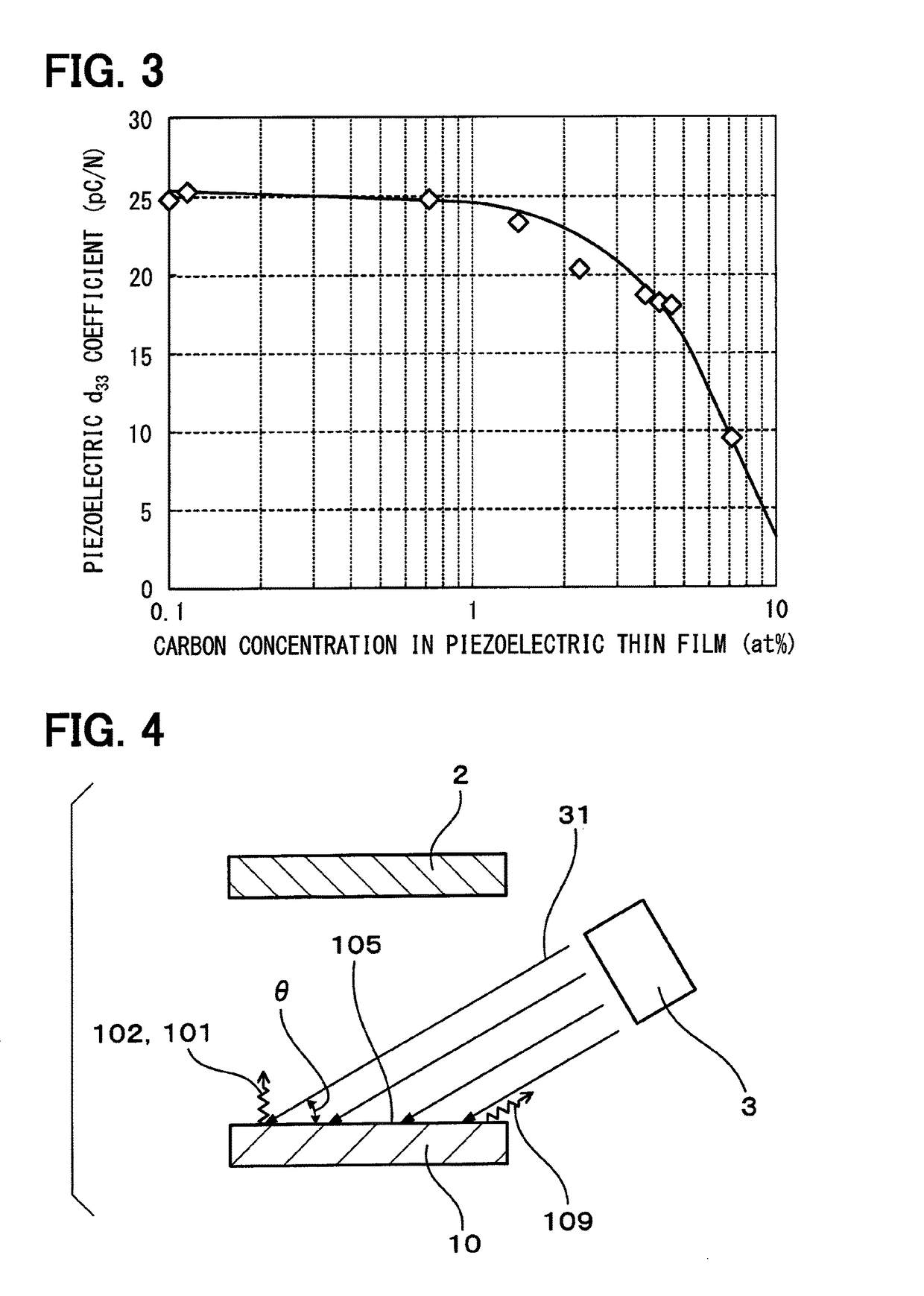
[0040]In the present example, piezoelectric thin films having different carbon atom (C) contents are produced, and the piezoelectric coefficients are evaluated.

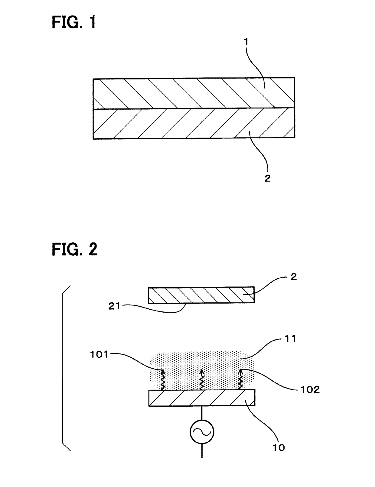
[0041]As shown in FIG. 1, a piezoelectric thin film 1 of the present example has been provided on a substrate 2 formed of silicon. The piezoelectric thin film 1 consists essentially of scandium aluminum nitride and contains a tiny amount of carbon.

[0042]To produce the piezoelectric thin film 1, a commercially available substrate formed of silicon and a commercially available alloy target material which was in the form of a plate and which consisted essentially of a scandium aluminum alloy (Sc0.45Al0.55 alloy) were prepared. The alloy target material was prepared by high-frequency induction heating using a carbon crucible, and the composition ratio of elements of scandium and aluminum was 0.45:0.55 (Sc:Al). In the present example, the...

modification 1

(Modification 1)

[0059]In Example 1, the piezoelectric thin films were prepared by a single-target sputtering step using alloy target materials each including a scandium aluminum alloy. However, a piezoelectric thin film can be produced also by a two-target sputtering step using an Sc target material consisting essentially of scandium and an Al target material consisting essentially of aluminum. In this case, a piezoelectric thin film can be produced in a similar manner as in Example 1, except that aluminum and scandium are sputtered simultaneously on a substrate from an Sc target material and an Al target material.

[0060]Carbon is included in the Sc target material, not in the Al target, in a two-target sputtering step like the step of the present modification. The carbon contaminates during the production of the Sc target like the alloy target materials in Example 1. Here, as demonstrated in Example 1, the carbon atomic content of the piezoelectric thin film consisting essentially o...

example 2

[0062]In the present example, a piezoelectric thin film consisting essentially of scandium aluminum nitride is produced by an ion irradiation sputtering step, where the sputtering is conducted by applying an ion beam to an opposing surface of an alloy target material at an oblique angle.

[0063]Specifically, an alloy target material 10 including a scandium aluminum alloy was provided with the opposing surface facing a substrate 2 as in Example 1 (see FIG. 4).

[0064]A silicon substrate similar to the silicon substrate of Example 1 can be used as the substrate 2. A scandium aluminum alloy target material having a carbon content of for example 5 at % or less, as in Example 1, may also be used as the alloy target material 10. Alternatively, however, an alloy target material having a carbon content exceeding 5 at % may also be used.

[0065]As shown in FIG. 4, an ion beam 31 including nitrogen ions was applied to an opposing surface 105 of the alloy target material 10 at an oblique angle using...


PUM

PropertyMeasurementUnit
pressureaaaaaaaaaa
pressureaaaaaaaaaa
temperatureaaaaaaaaaa

Abstract

A piezoelectric thin film is formed through sputtering and consists essentially of scandium aluminum nitride. The carbon atomic content is 2.5 at % or less. When producing the piezoelectric thin film, scandium and aluminum are sputtered simultaneously on a substrate from a scandium aluminum alloy target material having a carbon atomic content of 5 at % or less in an atmosphere where at least nitrogen gas exists. The sputtering may be conducted also by applying an ion beam on an opposing surface of the alloy target material at an oblique angle. Moreover, aluminum and scandium may be also sputtered simultaneously on the substrate from an Sc target material and an Al target material. As a result, a piezoelectric thin film which exhibits excellent piezoelectric properties and a method for the same can be provided.

Description

CROSS REFERENCE TO RELATED APPLICATIONS[0001]This application is a U.S. national stage of International Application No. PCT / JP2014 / 002697 filed on May 22, 2014 and is based on Japanese Patent Application No. 2013-115477 filed on May 31, 2013, the disclosures of which are incorporated herein by reference.TECHNICAL FIELD[0002]The present disclosure relates to a piezoelectric thin film consisting essentially of scandium aluminum nitride and a method for producing the same.BACKGROUND ART[0003]A piezoelectric thin film including scandium aluminum nitride (ScxAl1-xN; 0<x<1) is capable of exhibiting a higher piezoelectric coefficient for example than an aluminum nitride thin film and the like. Therefore, it is expected that a piezoelectric thin film will be applied to a surface acoustic wave (SAW) element, a light-emitting layer for a light-emitting diode (LED) having a wide emission wavelength range, a microelectromechanical systems (MEMS) element and the like.[0004]A piezoelectric ...

Claims


Application Information

Patent Timeline
Patent Type & Authority Patents(United States)
IPC IPC(8): H01L41/18H01L41/316H01L41/187C23C14/34C23C14/46C23C14/18C23C14/06H01L41/39C04B35/581H10N30/85H10N30/853H10N30/076H10N30/093
CPCH01L41/18C23C14/06C23C14/18C23C14/185C23C14/34C23C14/3464C23C14/46H01L41/187H01L41/316C23C14/0052C23C14/0641H10N30/853H10N30/076H10N30/04
Inventor TESHIGAHARA, AKIHIKOKANO, KAZUHIKOAKIYAMA, MORITONISHIKUBO, KEIKO
Owner DENSO CORP
Learn More