Scalable CVD film and nanomaterial synthesis

a cvd film and nanomaterial technology, applied in the direction of thin material processing, metallic material coating process, coating, etc., can solve the problems of limiting the application of batch process cvd systems for research and development, hindering the growth of undisturbed, and affecting the development of undisturbed

Active Publication Date: 2017-08-22
CVD EQUIP CORP
View PDF3 Cites 0 Cited by
  • Summary
  • Abstract
  • Description
  • Claims
  • Application Information

AI Technical Summary

Benefits of technology

[0014]It is a seventh objective of this invention to lower the production cost and development cost for scaling up CVD processing of flexible materials
[0021]It is contemplated that the substrate remounting method of the present invention can be retrofitted into existing CVD systems for increased production capacity, and that customized CVD system designs with optimized loading capacity in accordance with this invention, together with custom tuned CVD processes, can provide cost optimized production solutions for each given nano-structured material or surface modified flexible substrate manufacturing challenge.
[0022]Thus, this invention relates, at least in part, to CVD batch processing systems enclosing one or more flexible substrates with one or two-sided catalytic active surfaces that in total have a large usable surface area on which such nano-structured materials can be synthesized. Another aspect of this invention addresses economical CVD process solutions for surface modification of flexible substrates, such as increasing the corrosion resistance of steel foil by enriching its surface layer with suitable chemicals, e.g., Ni, Cr, C, to make such layer more “stainless steel-like”.

Problems solved by technology

In this regard, the lack of related economical production solutions has hindered commercialization efforts.
However, the gas porous material interferes with local surface processing, and hinders the growth of undisturbed, higher quality nano-structured materials like carbon nanotubes and silicon nanowires.
Additionally, the processing conditions developed with batch process CVD systems used for research and development (R&D) are typically not directly portable to roll-to-roll CVD systems, which then typically requires multiple generations of pilot system development prior to scale up to a production roll-to-roll CVD system.
This thus increases the capital cost, development risk and commercialization time frame of roll-to-roll CVD projects, often putting it out of reach for many smaller / startup corporations.
As a result, the scale up of large area CVD processed films and / or nano-structured material covered flat substrates has, in the past, only been implemented commercially on a selective basis for high volume applications.

Method used


Image

  • Scalable CVD film and nanomaterial synthesis
  • Scalable CVD film and nanomaterial synthesis
  • Scalable CVD film and nanomaterial synthesis

Examples


Embodiment Construction

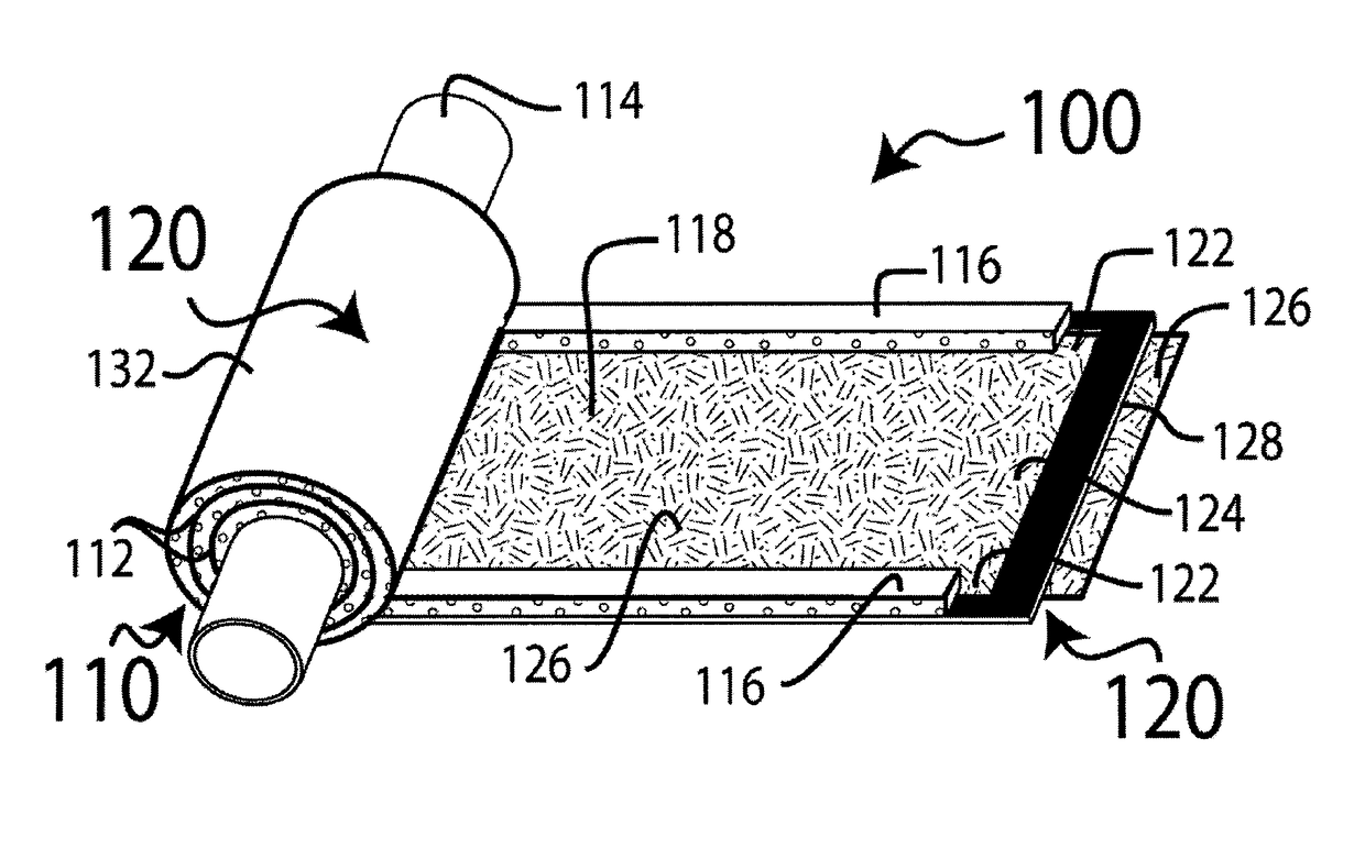
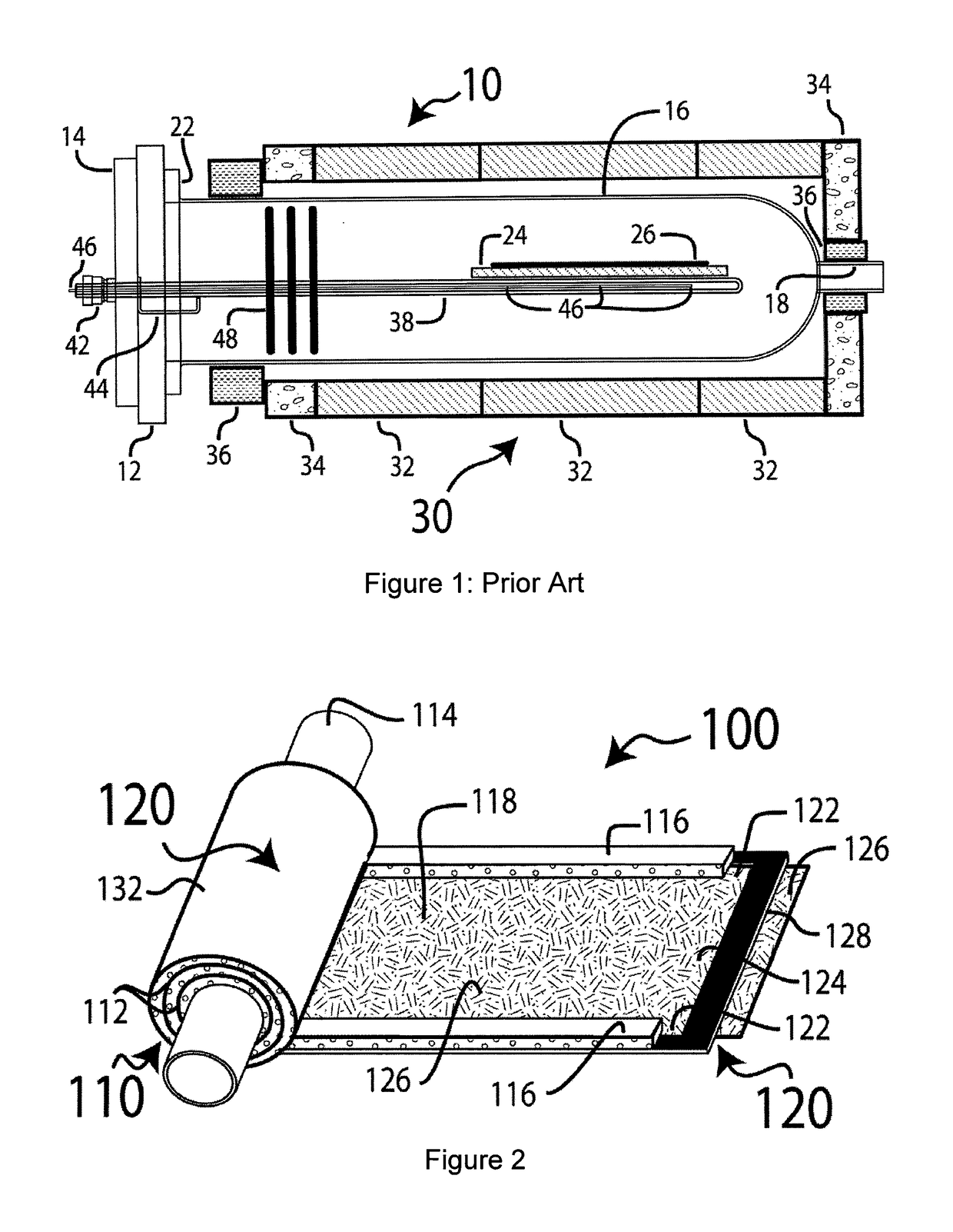
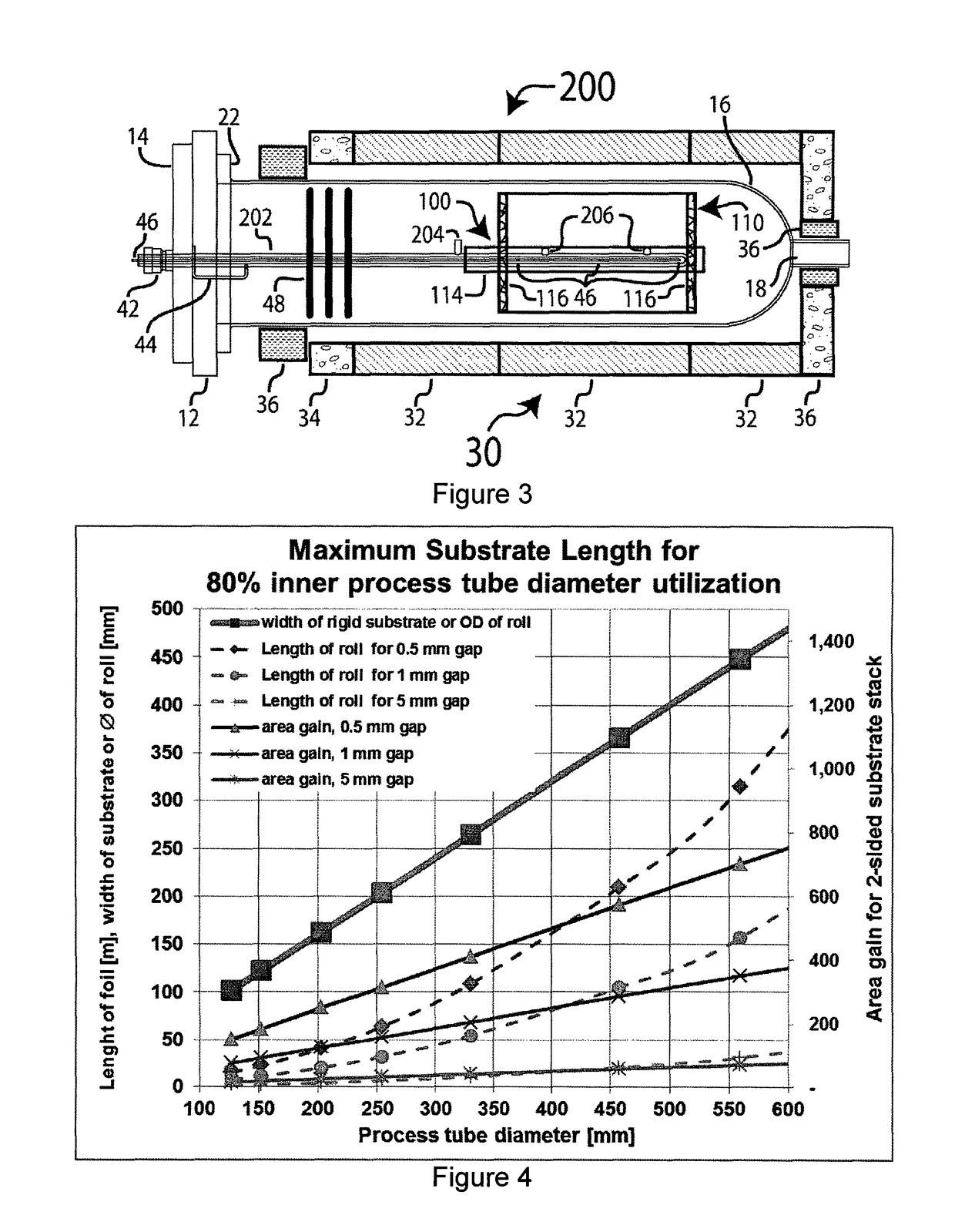
[0032]FIG. 1 shows the components of a prior art R&D CVD horizontal tube furnace system, which includes a heated process chamber 10. The chamber 10 includes a gas ring 12, an end cap 14 and a asymmetric process tube 16 with a narrowed down neck exhaust gas port 18 on one side and a flange 22 on the other side. The chamber 10 is formed by a sealed arrangement (i.e., with o-rings and cooling to protect the seals) of gas ring 12, process tube 16, end cap 14, and all respective entry and exhaust gas ports. The process tube 16 is surrounded (at least during part of the CVD processing time) by a resistive oven 30, which can have multiple individually controllable heating zones 32, insulating end zones 34, and optionally flexible and removable insulating structure 36, i.e., flexible insulating collars made from quartz fibers or ceramic wool, between the oven end zones 34 and the process tube 16. Various systems / methods (not shown) are used in prior art systems for injecting and distributin...


PUM

PropertyMeasurementUnit
thickaaaaaaaaaa
thickaaaaaaaaaa
thickaaaaaaaaaa

Abstract

The present invention relates to tools and system designs for chemical vapor deposition (CVD) systems and CVD synthesis used to deposit one or more thin film layers onto a flexible substrate or to grow nano-structured materials on large area flexible substrates and, more particularly, to scalable CVD coating and nanostructure manufacturing including CVD thin films and nano-structured materials such as nanotubes, nanowires and nanosheets.

Description

[0001]This application claims the benefit of U.S. Provisional Application No. 62 / 012,178, filed on Jun. 13, 2014.BACKGROUND OF THE INVENTION[0002]The present invention relates to substrate remounting and system designs for chemical vapor deposition (CVD) systems and CVD synthesis used to synthesize at least one layer or to grow at least one nano-structured material on at least one surface of a flexible substrate, and more particularly, to scalable thin film coating and nano-structured material manufacturing of products such as nanotubes, nanowires, and nanosheets.[0003]Those skilled in the art will recognize that there is an ongoing interest in economical solutions that enable the manufacturing in large volume of higher quality, nano-structured materials (e.g., in tube, fiber or wire format, such as 1-5 mm tall, 10-20 nm thick vertically aligned carbon nanotubes; 100-200 nm thick vertically aligned carbon nanofibers; 10-50 μm long, 50-100 nm thick random or vertically aligned silico...

Claims


Application Information

Patent Timeline
Patent Type & Authority Patents(United States)
IPC IPC(8): B32B3/00C23C16/458
CPCC23C16/458Y10T428/24777
Inventor STROBL, KARLHEINZ
Owner CVD EQUIP CORP
Why Eureka
Try Eureka