
Delayed fluorescence material and organic electroluminescence device

a technology of delayed fluorescence and electroluminescence device, which is applied in the direction of luminescent compositions, organic semiconductor devices, luminescent compositions, etc., can solve the problems of reducing light emission efficiency and forming exciplexes, and achieve high exciton forming efficiency, high external quantum efficiency, and high light emission efficiency.

Active Publication Date: 2017-10-10
KYULUX INC
View PDF32 Cites 2 Cited by
  • Summary
  • Abstract
  • Description
  • Claims
  • Application Information

AI Technical Summary

Benefits of technology

[0044]In the delayed fluorescence material of the invention an acceptor compound and a donor compound satisfying the specific conditions are mixed to form an exciplex, and is therefore characterized in that its light emission efficiency is extremely high. The organic electroluminescence device using the delayed fluorescence material of the invention has a high exciton forming efficiency and a high external quantum efficiency.

Problems solved by technology

On the other hand, Patent References 4 and 5 say that forming an exciplex reduces light emission efficiency.

Method used


Image

  • Delayed fluorescence material and organic electroluminescence device
  • Delayed fluorescence material and organic electroluminescence device
  • Delayed fluorescence material and organic electroluminescence device

Examples


example 1

(1) Production of Samples 1 to 3

[0111]Samples 1 to 3 were produced according to the method mentioned below.

[Sample 1]

[0112]On a silicon substrate, 4,4′,4″-tris[3-methylphenyl(phenyl)amino]triphenylamine (m-MTDATA: compound 8c) was vacuum-deposited in a thickness of 100 nm to produce a sample 1.

[Sample 2]

[0113]On a silicon substrate, tris(2,4,6-trimethyl-3-(pyridin-3-yl)phenyl)borane (3TPYMB: compound 1b) was vacuum-deposited in a thickness of 100 nm to produce a sample 2.

[Sample 3]

[0114]On a silicon substrate, 3TPYMB doped with 50 mol % m-MTDATA was co-deposited in a thickness of 100 nm to produce a sample 3.

(2) Analysis of Sample 1 and Sample 2

[Determination of Excited Triplet Energy]

[0115]Using a streak camera, the phosphorus spectra of the sample 1 and the sample 2 were taken. As the excitation light source, used as a nitrogen gas laser at a wavelength of 337 nm. Using a cryostat, the sample was cooled to a temperature of 10K, and analyzed. In the phosphorus spectrum thus taken, ...

example 2

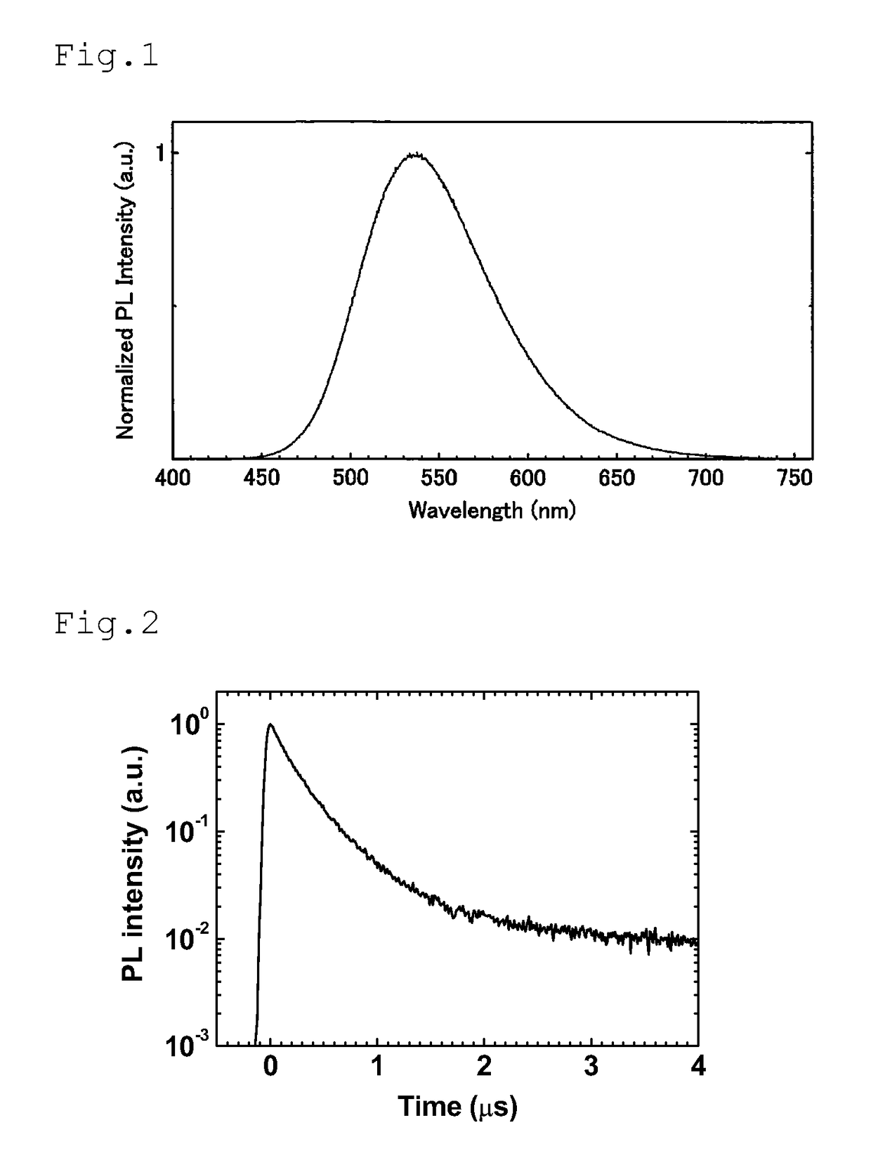
[0124]Samples were produced according to the same process as in Example 1 except that SPPO1 (compound 2) was used as the acceptor compound in place of 3TPYMB (compound 1b). The excited triplet energy of the sample 2 (SPPO1) was 2.9 eV, the energy level of HOMO was 6.5 eV, and the energy level of LUMO was 2.7 eV. The excited singlet energy of the exciplex of the sample 3 was 2.4 eV. FIG. 3 shows the time-resolved PL spectrum.

examples 3 to 5

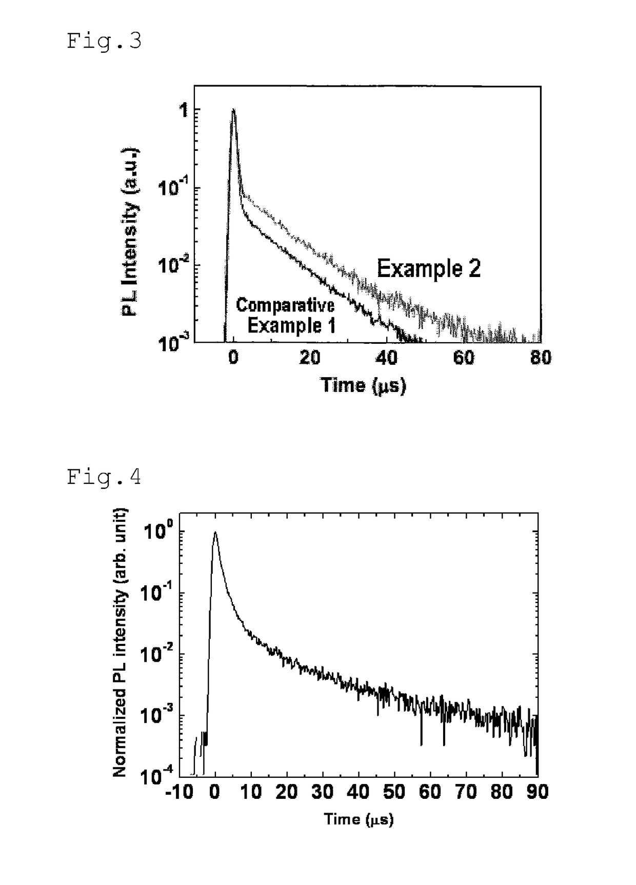
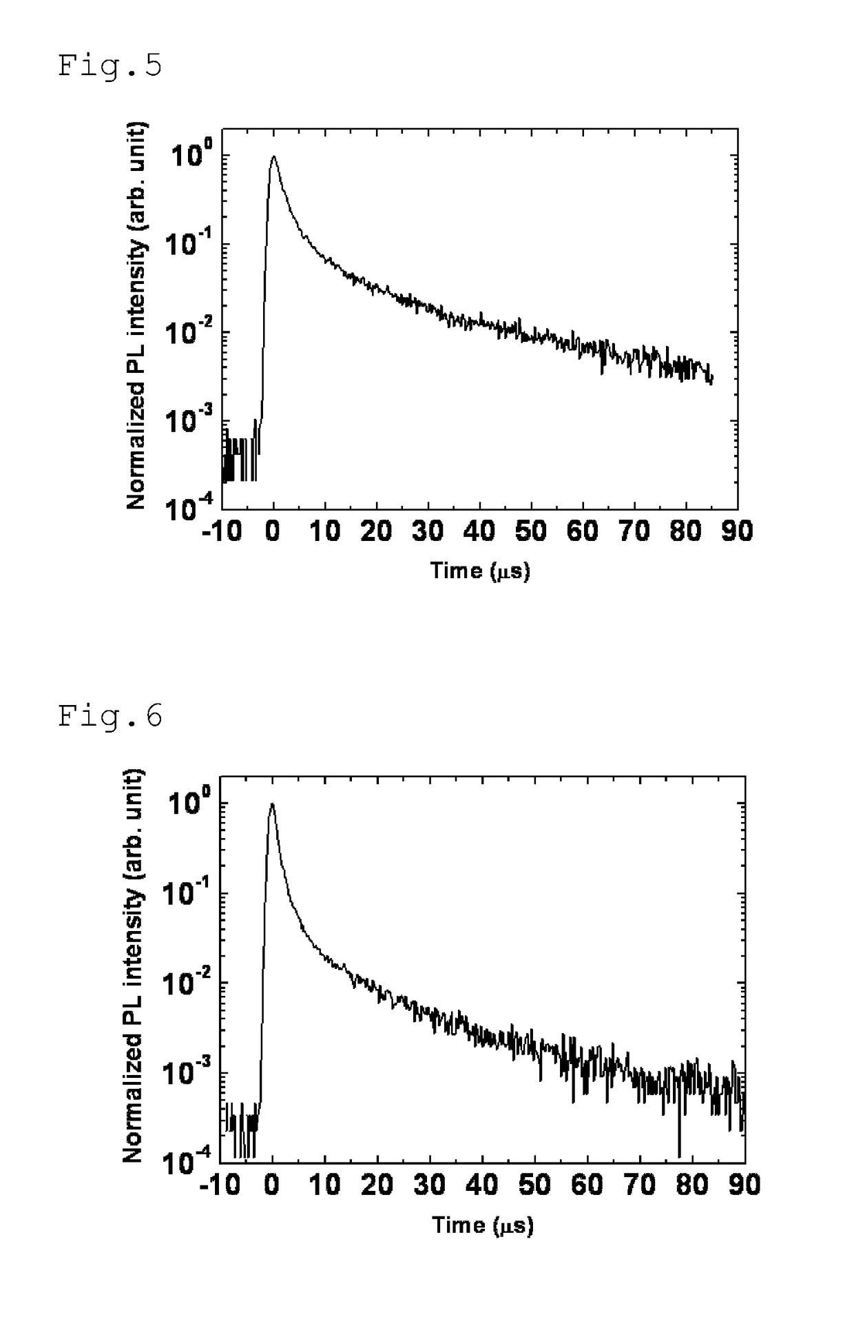
[0128]Samples were produced and measured according to the same process as in Example 1 except that the acceptor and the donor shown in Table 3 were used. The results are shown in Table 3 and FIGS. 4 to 6.

[0129]

TABLE 3time-resolvedCompound No.Measured DataPLAcceptorDonorT1AT1DLUMOAHOMODS1T1A − S1T1D − S1spectrumExample 11b8c2.82.63.45.12.30.50.3FIG. 2Example 228c2.92.62.75.12.40.50.2FIG. 3Comparativet-BuPBD8c2.42.62.45.12.30.10.3FIG. 3Example 1Example 31b9g2.82.73.45.32.40.40.3FIG. 4Example 41b8a2.82.63.45.22.30.50.3Fog. 5Example 51b9c2.82.73.45.32.50.30.2FIG. 6


PUM

PropertyMeasurementUnit
thicknessaaaaaaaaaa
thicknessaaaaaaaaaa
LUMOaaaaaaaaaa

Abstract

A delayed fluorescence material containing a mixture of an acceptor compound and a donor compound that satisfies the following formulae (1) to (4):T1A−S1>0.2 eV  (1)T1D−S1≧0.2 eV  (2)|LUMOA|>2.0 eV  (3)|HOMOD|≦5.3 eV  (4)wherein T1A represents the excited triplet energy of the acceptor compound; T1D represents the excited triplet energy defined of the donor compound; S1 represents the excited singlet energy of the exciplex; LUMOA represents the energy level of LUMO of the acceptor compound; and HOMOD represents the energy level of HOMO of the donor compound.

Description

CROSS-REFERENCE TO RELATED APPLICATIONS[0001]The present application claims the benefit of priority from Japanese Patent Application No. 2011-42965, filed on Feb. 28, 2011, the contents of which are herein incorporated by reference in their entirety.BACKGROUND OF THE INVENTION[0002]Field of the Invention[0003]The present invention relates to a novel delayed fluorescence material and to an organic electroluminescence material using the delayed fluorescence material.[0004]Description of the Related Art[0005]Studies for increasing the light emission efficiency of organic electroluminescent devices (organic EL devices) are being made actively. In particular, various studies of developing novel light-emitting materials for attaining more efficient light emission are being made. Among them, a delayed fluorescence material for delayed light emission is expected as a material that has a latent possibility of drastically increasing light emission efficiency. Until now, some delayed fluoresce...

Claims


Application Information

Patent Timeline
Patent Type & Authority Patents(United States)
IPC IPC(8): H01L51/54C09K11/06H05B33/14H01L51/00H01L51/50
CPCC09K11/06H01L51/0059H05B33/14C09K2211/1007H01L2251/552C09K2211/1014C09K2211/1059H01L51/5012H01L2251/308C09K2211/1011H10K85/631H10K50/11H10K2101/30H10K2102/103H10K2101/20
Inventor ADACHI, CHIHAYAGOUSHI, KENICHIYOSHIDA, KOU
Owner KYULUX INC
Learn More