System and method for designing system on chip (SoC) circuits through artificial intelligence and reinforcement learning

a technology of reinforcement learning and system on chip, applied in the field of systems/systems for designing integrated circuits, can solve the problems of not having a system and method available, design does not teach about implementing an ai framework, and the process of converting a design flow (of a soc circuit) into a physical design is not free from (design related) errors, so as to reduce the complexity of the decision-making process

Active Publication Date: 2017-10-17
ALPHAICS CORP
View PDF2 Cites 77 Cited by
  • Summary
  • Abstract
  • Description
  • Claims
  • Application Information

AI Technical Summary

Benefits of technology

[0022]The embodiments herein discloses a SoC design framework embedded with artificial intelligence and configured to adapt and implement reinforcement learning techniques. The SoC design framework disclosed in the embodiments herein is designed to reduce the complexity in the decision making process associated with design of SoC circuits. The decisions associated with the designing of SoC circuits are multitude and typically heterogeneous in nature. The SoC design framework of the embodiments herein is configured to generalize the multitude of heterogeneous decisions into a plurality of generalized, homogenous decisions, which are in turn utilized to finalize and implement the design for the SoC circuits. The SoC design framework disclosed in the embodiments herein is designed to utilize a combination of artificial intelligence and reinforcement learning principles to arrive at optimal decisions regarding the design and implementation of SoC circuits.

Problems solved by technology

Further, the process of converting a design flow (of a SoC circuit) into a physical design is not free from (design related) errors due to a manual implementation and fragmented nature (of the corresponding design flow).
Typically, functional verification (for determining whether the logic design of the SoC circuit confirms to the design specification), which forms a critical part of the transformation from design flow (of a SoC circuit) to physical design, demands the largest pool of resources (in terms of time, manpower inter-alia), due to the complexity of the SoC circuit design as well as the enormity of possible test cases / test scenarios necessary to completely verify the SoC circuit design in its entirety.
At present, there is no system and method available and exist for generalization and learnability of data generated in chip designing process.
The existing process of SoC chip design does not teach about implementing an AI framework into the manual chip design process.

Method used


Image

  • System and method for designing system on chip (SoC) circuits through artificial intelligence and reinforcement learning
  • System and method for designing system on chip (SoC) circuits through artificial intelligence and reinforcement learning
  • System and method for designing system on chip (SoC) circuits through artificial intelligence and reinforcement learning

Examples


Embodiment Construction

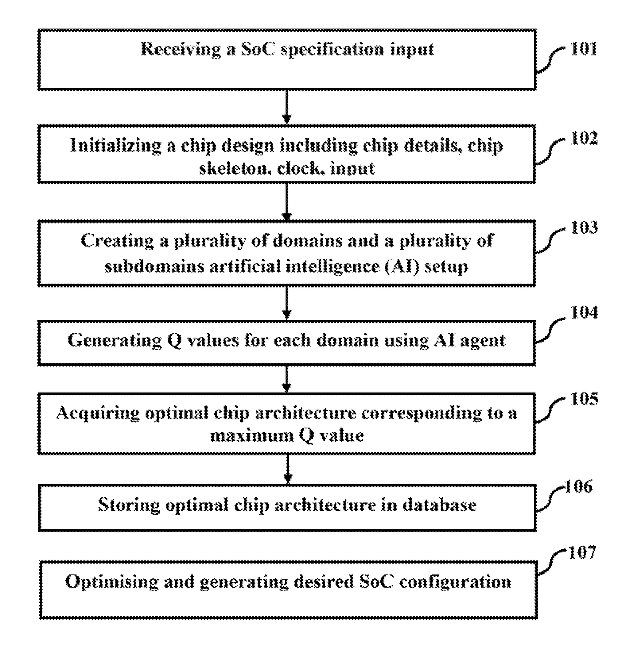
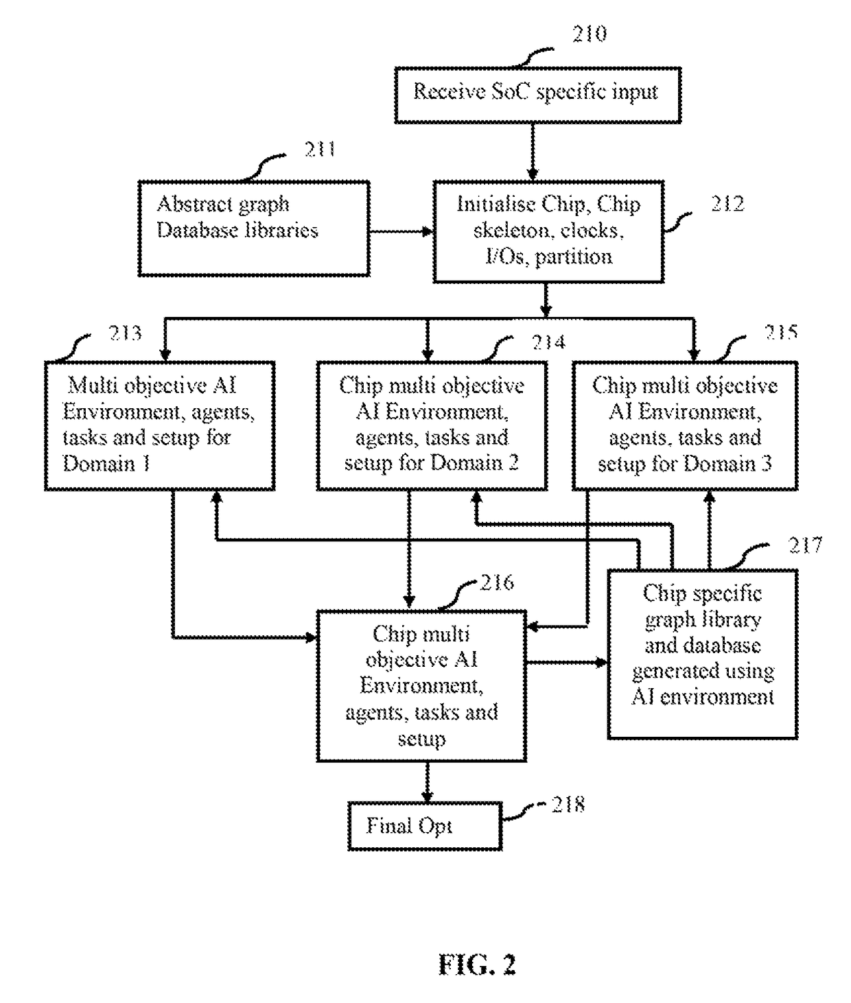
[0012]An object of the embodiments herein is to develop a SoC design framework implemented on the basis of artificial intelligence.

[0013]Another object of the embodiments herein is to provide a SoC design framework that employs reinforcement learning techniques to improve the design and implementation of SoC circuit design.

[0014]Yet another object of the embodiments herein is to provide an artificial intelligence based framework optimized for SoC design and implementation.

[0015]Yet another object of the embodiments herein is to provide a method for learning and inferencing from SoC design that can be used for future designing of SoC.

[0016]Yet another object of the embodiments herein is to provide a SoC design framework that automates the process of SoC design and implementation.

[0017]Another object of the embodiments herein is to provide a SoC design framework that is flexible and modular in construction.

[0018]Yet another object of the embodiments herein is to provide a SoC design f...


PUM


Abstract

The embodiments herein discloses a system and method for designing SoC using AI and Reinforcement Learning (RL) techniques. Reinforcement Learning is done either hierarchically in several steps or in a single-step comprising environment, tasks, agents and experiments, to have access to SoC (System on a Chip) related information. The AI agent is configured to learn from the interaction and plan the implementation of a SoC circuit design. Q values generated for each domain and sub domain are stored in a hierarchical SMDP structure in a form of SMDP Q table in a big data database. An optimal chip architecture corresponding to a maximum Q value of a top level in the SMDP Q table is acquired and stored in a database for learning and inference. Desired SoC configuration is optimized and generated based on the optimal chip architecture and the generated chip specific graph library.

Description

CROSS-REFERENCE TO RELATED APPLICATION[0001]The embodiments herein claim the priority of the U.S. Provisional Patent Application Ser. No. 62 / 443,803 filed on Jan. 8, 2017, with the title, “COMPUTER IMPLEMENTED SYSTEM FOR DESIGNING SYSTEM ON CHIP CIRCUITS AND METHOD THEREOF”, and the contents of which is included entirely as reference herein.BACKGROUND[0002]Technical Field[0003]The embodiments herein is related to apparatuses / systems for designing Integrated Circuits (IC). The embodiments herein is particularly related to apparatuses / systems for designing IC such as system on chip (SoC). The embodiments herein is more particularly related to a system and method for designing system on chip (SoC) using artificial intelligence (AI) and reinforcement learning techniques.[0004]Description of Related Art[0005]System on Chip (SOC) is an integrated circuit (IC) that integrates all the components of an electrical / electronic system into a single chip. The integrated circuit typically comprise...

Claims


Application Information

Patent Timeline
Patent Type & Authority Patents(United States)
IPC IPC(8): G06F17/50
CPCG06F17/504G06F17/505G06F30/27G06F2115/02G06F30/32G06F30/327G06F30/3323
Inventor NAGARAJA, NAGENDRA
Owner ALPHAICS CORP
Why Eureka
Try Eureka