Systems, methods and apparatus for enabling high voltage circuits

a high-voltage circuit and system technology, applied in pulse generators, semiconductor/solid-state device testing/measurement, pulse techniques, etc., can solve problems such as unsatisfactory leakage currents, and achieve the effect of reducing the back gate effect in the silicon on insulator (soi) structur

Active Publication Date: 2017-12-19
PSEMI CORP
View PDF37 Cites 18 Cited by
  • Summary
  • Abstract
  • Description
  • Claims
  • Application Information

AI Technical Summary

Benefits of technology

[0008]According to a fifth aspect of the present disclosure, a method for reducing a back gate effect in a silicon on insulator (SOI) structure is presented, the method comprising: forming a first silicon region in a thin silicon layer of the SOI structure, the first silicon region configured to be coupled to a first voltage having a high level equal to or higher than 10 V; forming a second silicon region, isolated from the first silicon region, in the thin silicon layer, the second silicon region configured to be coupled to a second voltage having a high level equal to or lower than 3 V; forming a control structure configured to affect a coupling between the thin silicon layer and a silicon substrate of the SOI structure; coupling the first voltage to the first silicon region and the second voltage to the second silicon region; coupling the substrate to a reference potential; based on the forming and the coupling, controlling one or both of: a potential at a first surface region of the substrate proximate the first silicon region, and a potential at a second surface region of the substrate proximate the second silicon region, and based on the controlling, reducing the back gate effect in one or both of the first silicon region and the second silicon region.

Problems solved by technology

For HV circuits, the buried oxide layer (BOX) and the grounded substrate can cause a back gate effect in which the substrate serves as a gate that can change the potential of the electronic elements of the HV circuits in the upper Si layer causing undesirable leakage currents.

Method used


Image

  • Systems, methods and apparatus for enabling high voltage circuits
  • Systems, methods and apparatus for enabling high voltage circuits
  • Systems, methods and apparatus for enabling high voltage circuits

Examples


Embodiment Construction

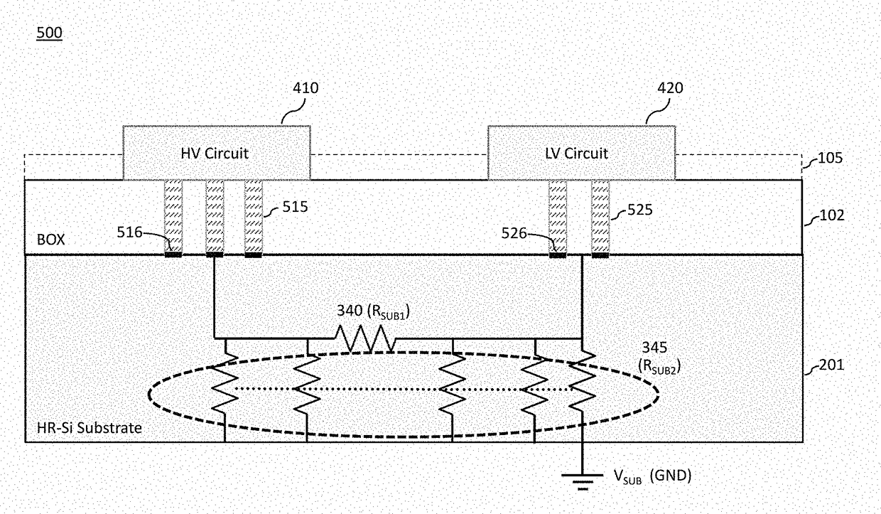
[0026]The majority of integrated circuits, ICs, used in such applications as cell phones, personal computers and consumer electronics, operate at relatively low voltages, typically below 5 V and often below 3 V. High voltages, which in the present disclosure are defined as any DC voltage above 5 V, are becoming more prevalent due to the efficiency of storing energy at these voltages, especially in batteries. It is not uncommon to find battery storage such as that in hybrid cars or in solar power systems to be in the 10-100 V range.

[0027]Such high voltages can be controlled directly or can be reduced to lower voltages for control by standard ICs. For example, in either a hybrid car or solar powered house, the high voltage coming from a battery or solar panel must be reduced from 10-100 V, to 1-3 V to be used by consumer electronics ICs.

[0028]Conversion from high to low voltage is often performed by DC-DC converters due to their small size, high efficiency and flexibility. It is desir...


PUM


Abstract

Systems, methods and apparatus for coexistence of high voltage and low voltage devices and circuits on a same integrated circuit fabricated in silicon-on-insulator (SOI) technology are described. In particular, techniques for mitigating back gate effects are described, including using of resistive and/or capacitive couplings to control surface potentials at regions of a substrate used for the SOI fabrication proximate the high voltage and low voltage devices and circuits. In one case, an N-type implant is used to provide a high potential differential with respect to a substrate potential.

Description

CROSS REFERENCE TO RELATED APPLICATIONS[0001]The present application may be related to U.S. application Ser. No. 14 / 661,848 entitled “Level Shifter”, filed on Mar. 18, 2015, issuing as U.S. Pat. No. 9,484,897 on Nov. 1, 2016, which is herein incorporated by reference in its entirety. The present application may also be related to U.S. application Ser. No. 14 / 964,412 entitled “S-Contact for SOI”, filed on Dec. 9, 2015 which is herein incorporated by reference in its entirety.BACKGROUNDTechnical Field[0002]Various embodiments described herein relate generally to integrated circuits, ICs, and in particular to SOI ICs handling voltages higher than standard digital control voltages.Description of Related Art[0003]Integrated circuits, ICs, control voltages and currents in semiconductor substrates, of which there are many types. Si (silicon) is the most common substrate and a subset of Si substrates, silicon on insulator, SOI, is also widely used. In SOI, a buried insulator layer (buried o...

Claims


Application Information

Patent Timeline
Patent Type & Authority Patents(United States)
IPC IPC(8): H01L27/12H01L29/16H01L23/538H01L21/66H01L21/84H01L29/10H01L29/06H03K3/356
CPCH01L27/1203H01L29/0649H01L29/1095H01L21/84H01L22/12H01L29/16H01L23/5386H03K3/356104H01L29/78603H01L27/1218H01L23/535H01L21/743
Inventor ABESINGHA, BUDDHIKAWILLARD, SIMON EDWARDDUVALLET, ALAINGREEN, MERLINKUMARASAMY, SIVAKUMAR
Owner PSEMI CORP
Why Eureka
Try Eureka