

Semiconductor wafer, semiconductor device diced from semiconductor wafer, and method for manufacturing semiconductor device
a semiconductor wafer and semiconductor technology, applied in the field of semiconductor wafers, can solve problems such as cracks or the like, and achieve the effects of reducing the expansion of cracks, surface chipping, and film peeling, and improving the yield of diced semiconductor devices
- Summary
- Abstract
- Description
- Claims
- Application Information
AI Technical Summary
Benefits of technology
Problems solved by technology
Method used
Image

Examples
first embodiment
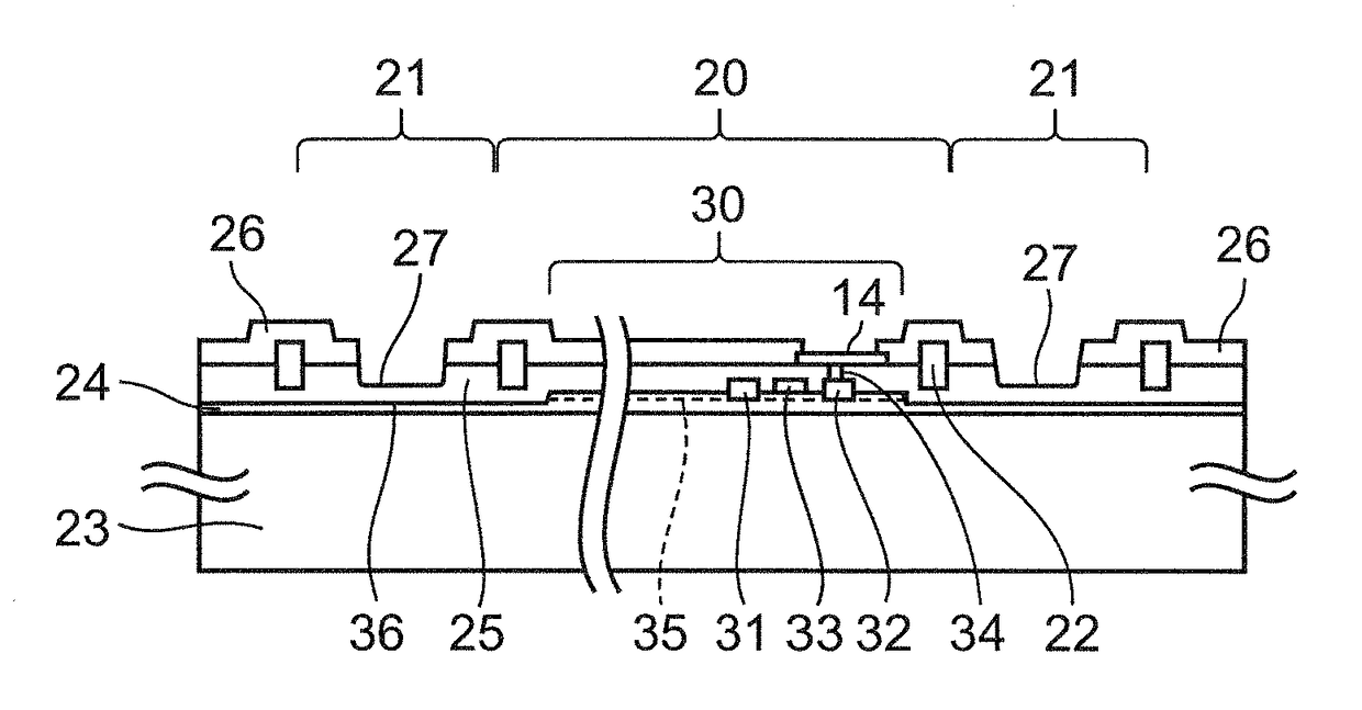
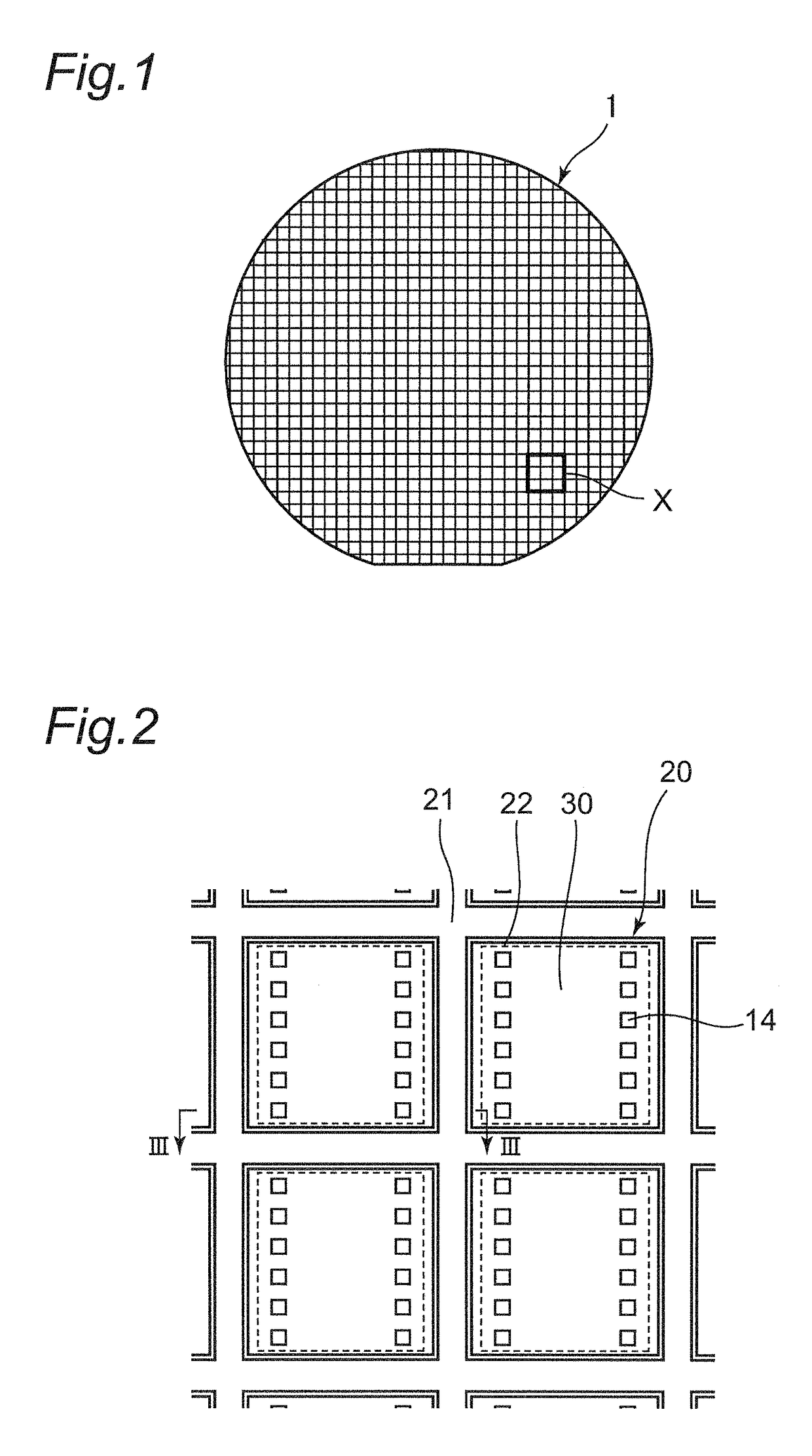
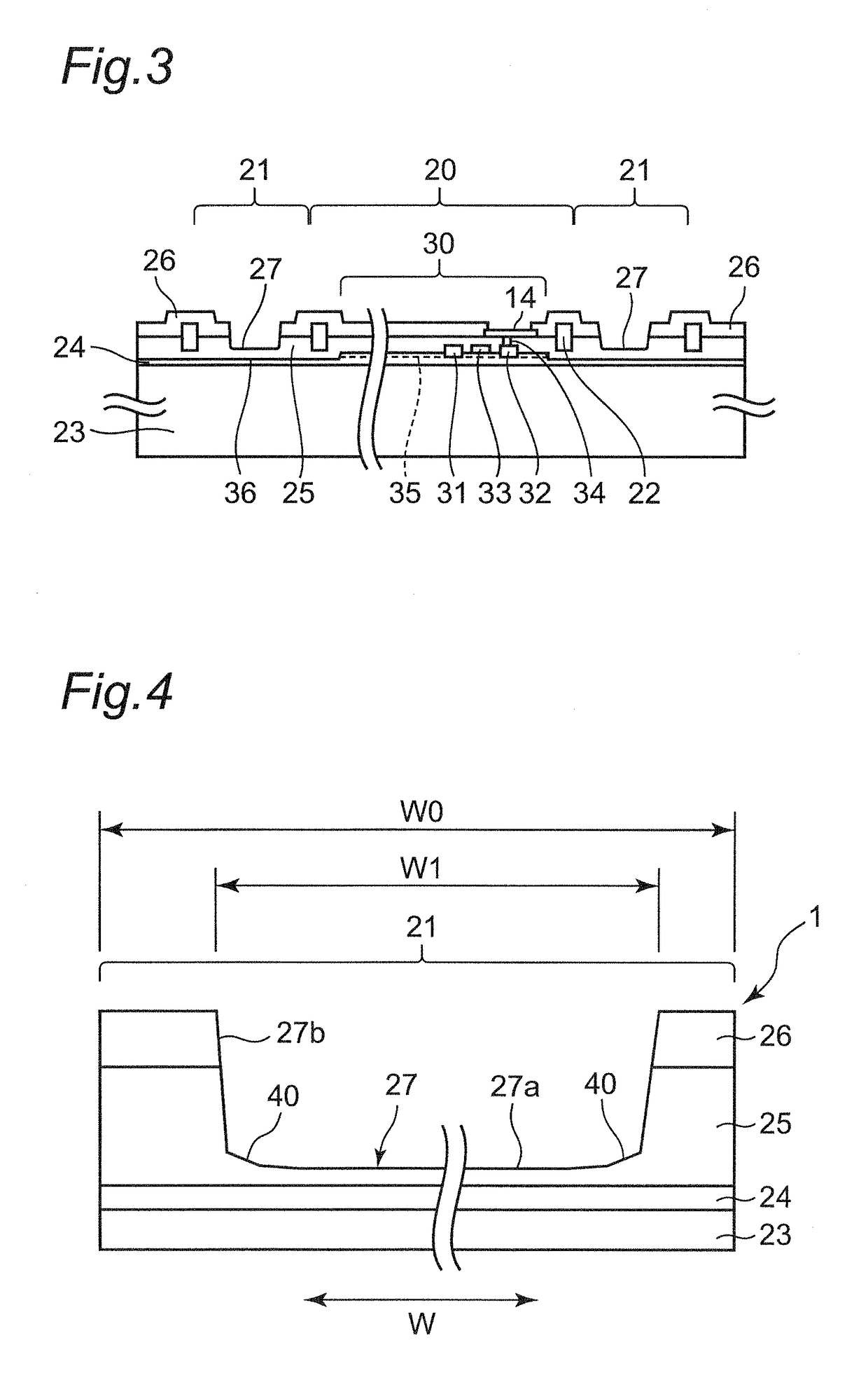
[0059]As shown in FIG. 1 and FIG. 2, a semiconductor wafer 1 of the first embodiment of the present invention is provided with a plurality of element regions 20 and a dicing region 21 which is provided in a lattice form so as to partition the element regions 20. Each of the element regions 20 is provided with a semiconductor element 30 (a circuit portion), bonding pads 14 which are provided on the semiconductor element 30, and a metal ring 22 which is provided so as to surround the semiconductor element 30. The semiconductor element 30 is a GaN type hetero-junction field effect transistor (HFET).
[0060]Here, a semiconductor device 70 diced from the semiconductor wafer 1 described above is formed by the element region 20 and a part of the dicing region 21 on the periphery of the element region 20.
[0061]As shown in FIG. 3, the semiconductor element 30 described above has a substrate 23 and a GaN type semiconductor film 24 which is laminated on the substrate 23. In the first embodiment,...
second embodiment
[0099]As shown in FIG. 15, in a semiconductor wafer 101 of the second embodiment, the dielectric film 25 of the semiconductor wafer 1 in the first embodiment is formed of multiple film layers of two layers formed of first and second dielectric films 49 and 50. Here, the same numbers are given to the same constituent portions as the first embodiment described above and the description of the first embodiment applies thereto.
[0100]As a dielectric film 125 in the semiconductor wafer 101 of the second embodiment, a SiN film with a film thickness of 2.0 μm or less produced by p-CVD is used, for example, as the first dielectric film 49 and a SiO2 film with a film thickness of 2.0 μm or less produced by p-CVD is used as the second dielectric film 50.
[0101]Here, the relationship between the film thickness of the second dielectric film 50 and the expansion of the cracks P at the time of blade dicing was examined in a case where the film thickness of the first dielectric film 49 was 0.75 μm. ...
third embodiment
[0108]Although not shown in the diagram, a semiconductor wafer 201 of the third embodiment is formed by a dielectric film 225 which is formed by further multi-layering the dielectric film 125 in the second embodiment. Here, the same numbers are given to the same constituent portions as the first and second embodiments described above and the description of the first and second embodiments applies thereto.
[0109]The dielectric film 225 of the semiconductor wafer 201 of the third embodiment has a configuration in which 6 layers of a SiN film (for example, a film thickness of 0.17 μm), a SiO2 film (for example, a film thickness of 0.15 μm), a SiN film (for example, a film thickness of 0.25 μm), a SiO2 film (for example, a film thickness of 0.75 μm), a SiN film (for example, a film thickness of 0.25 μm), and a SiO2 film (for example, a film thickness of 0.93 μm) are laminated in order.
[0110]Here, regarding the semiconductor wafer 201 described above, as a comparative example, using a sem...
PUM
 Abstract
Description
Claims
Application Information