

Joint structure for metal pillars
a joint structure and metal pillar technology, applied in the field of joint structure, can solve the problem of low bonding reliability of the joint structur
- Summary
- Abstract
- Description
- Claims
- Application Information
AI Technical Summary
Benefits of technology
Problems solved by technology
Method used
Image

Examples
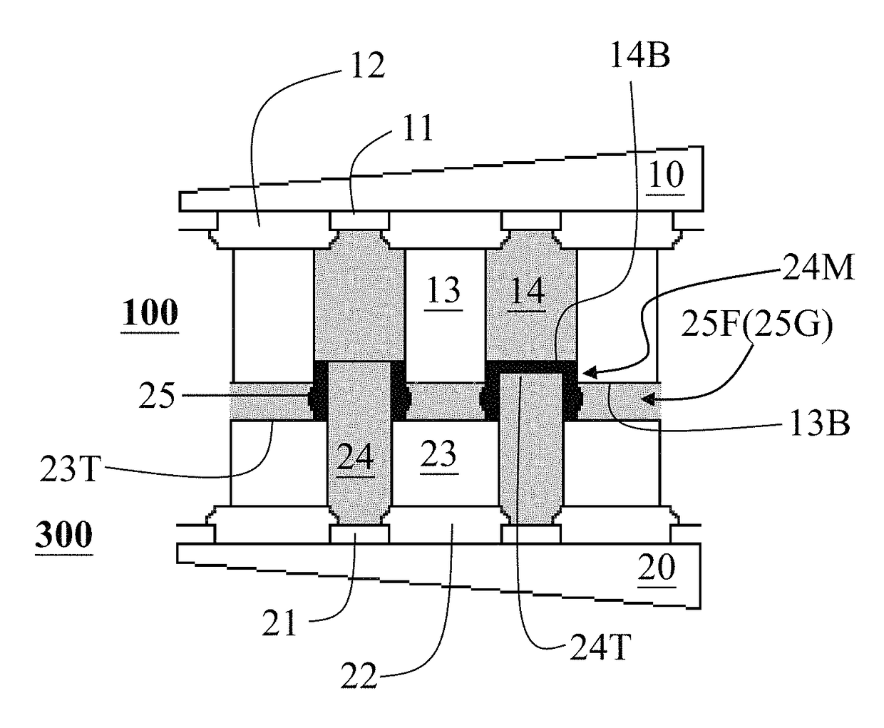
first embodiment
[0016]A first embodiment shows the connection metal block is formed by electroless deposition after matching the female structure to the male structure.
second embodiment
[0017]A second embodiment shows the connection metal block is a solder joint. The solder joint is formed by reflow a solder layer which is filled by screed printing process.
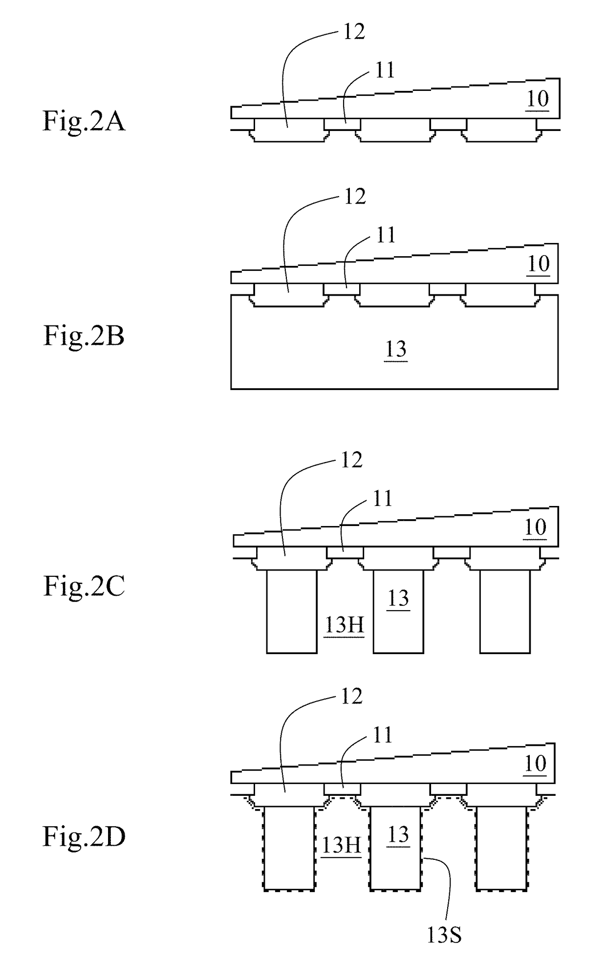
[0018]FIGS. 2A˜3B show a process for fabrication of metal pillars.
[0019]FIG. 2A shows
[0020]Preparing a first electronic component 10 which comprises a plurality of metal pads 11 formed on a bottom side. A passivation layer 12 is formed on a bottom side of the plurality of first metal pads 11. A bottom surface of each metal pad 11 is exposed from bottom side of the passivation layer 12.
[0021]FIG. 2B shows
[0022]Forming a photoresist layer 13 on a bottom surface of the plurality of metal pads 11.
[0023]FIG. 2C shows
[0024]Forming a plurality of holes 13H from a bottom side of the photoresist layer 13. A bottom surface of each metal pad 11 is exposed in a corresponding hole 13H.
[0025]FIG. 2D shows
[0026]Forming seed layer 13S on the surface of each hole 13H and on the bottom surface of each exposed metal pad 11.
[0027]FI...
PUM
| Property | Measurement | Unit |
|---|---|---|
| diameter | aaaaa | aaaaa |
| joint structure | aaaaa | aaaaa |
| diameter | aaaaa | aaaaa |
Abstract
Description
Claims
Application Information