
Superconductor

Inactive Publication Date: 2000-08-08
PANASONIC CORP
View PDF6 Cites 3 Cited by
  • Summary
  • Abstract
  • Description
  • Claims
  • Application Information

AI Technical Summary

Benefits of technology

The superconductor of this invention is essentially characterized in that a superconductive film is formed on a metal buffer film. The superconductive film is produced from the sputtering target which is made by breaking down its bare material into very fine powder and depositing such powdery target on a substrate, so that the composition of the formed superconductor film is essentially homogeneous as compared with the conventional sintered materials. Also, the superconductive film is homogeneously deposited and it becomes dense and flat on a metal film. Therefore, the present invention can not only realize an extraordinarily high quality superconductor but also increase the potential number of usable substrates, making it possible to obtain a film structure suitable for realizing various types of superconductor devices having superconductive films.

Problems solved by technology

However, with the present technical level, these oxide superconductive materials can only be produced by a sintering process, so that these supercondutive materials are available only in the form of powders or blocks of ceramics.
It has been, however, very difficult with the conventional technique to obtain a desired film or wire from these materials because of the poor reproducibility and a lack of reliability of their superconductive properties when they are made into a film or wire.

Method used


Image

  • Superconductor
  • Superconductor
  • Superconductor

Examples


embodiments

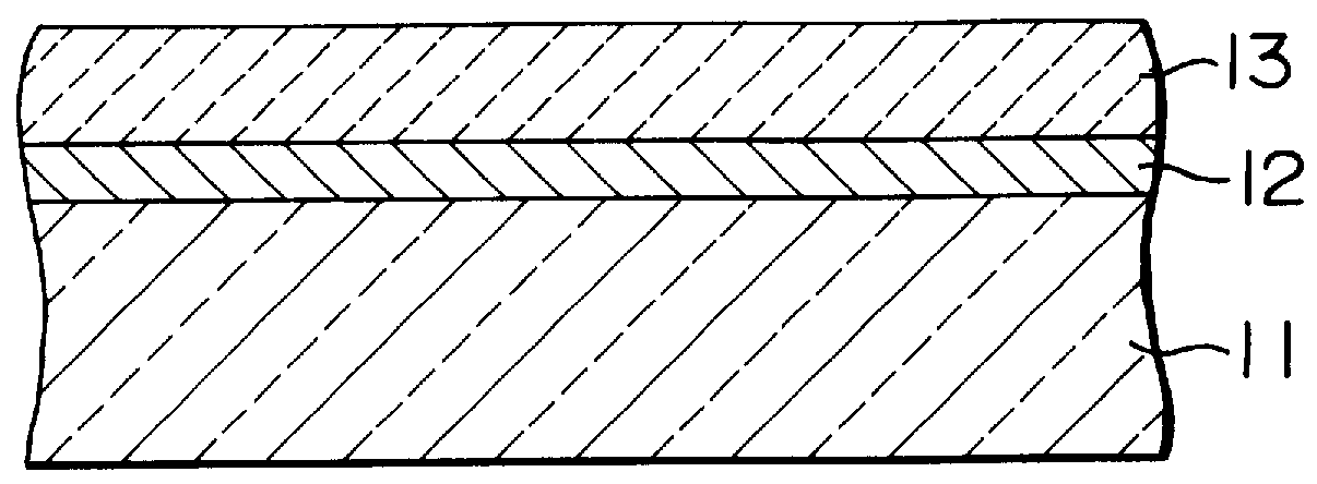
By using sapphire single crystal R plane as substrate 11 and a Pt plate as target, a Pt film 12 was deposited on the substrate by DC planar magnetron sputtering as shown in FIG. 1. Deposition was carried out at a sputtering power of 300 V.times.30 mA by using Ar gas pressurized to 8 Pa and maintaining the substrate temperature at 250.degree.-500.degree. C. to form a 0.1 .mu.m thick film. This Pt film was polycrystalline. On this Pt film 12 was deposited a compound film 13 by high frequency planer magnetron sputtering using sintered ErBa.sub.2 Cu.sub.4.sup...sub.5.sup.O.sub.8 as target. This sputtering deposition of compound film 13 was carried out under Ar gas pressure of 0.5 Pa at a sputtering power of 150 W for a period of one hour by maintaining the substrate temperature at 700.degree. C. to form a 0.5 .mu.m thick film.

This film showed a room-temperature resistance of 600 .OMEGA. and a superconducting transition temperature of 88 K.

Film formation on a glass coated substrate is de...


PUM

PropertyMeasurementUnit
Temperatureaaaaaaaaaa
Electrical resistanceaaaaaaaaaa
Superconductivityaaaaaaaaaa

Abstract

Excellent films of a high Tc superconductor are easily produced on metal coated substrates at a temperature below 700 DEG C. These metal buffer films are made of Pt, Au, Ag, Pd, Ni or Ti. The film superconductivity is significantly improved by the metal buffer layer. Since it is easy to form this metal coating on a substrate, the invention can increase the potential number of usable substrates such as fibers, amorphous solids or semiconductors.

Description

BACKGROUND OF THE INVENTIONThis invention relates to a superconductor, more particularly to a compound film superconductor.A-15 type binary (two-element) compounds such as niobium nitride (NbN) and niobium germanide (Nb.sub.3 Ge) had been known as high Tc superconductors, but the superconducting transition temperature of these materials was only about 24.degree. K. at highest. Perovskite type ternary (three-element) compounds have been expected to show higher transition temperatures, and a Ba.dbd.La.dbd.Cu--O high-Tc-superconductor has been proposed (J. B. Bendorz and K. A. Muller, Zetschrift Fur Physik B-Condensed Matter, 64, 189-193, 1986).Recently it was reported that Y.dbd.Ba.dbd.Cu--O type compounds could form superconductors with even higher transition temperatures than those of prior ones (M. K. Wu et al, Physical Review Letters, Vol. 58, No. 9, 908-910, 1987).The superconducting mechanism of the Y.dbd.Ba--Cu--O type materials is not yet definitely known, but there is a possi...

Claims


Application Information

Patent Timeline
IPC IPC(8): H01L39/24
CPCH01L39/2435H01L39/2458H01L39/2461Y10S428/93Y10T428/265Y10S428/901Y10S505/701Y10S505/702Y10S505/703Y10S505/704Y10T428/31678H10N60/0408H10N60/0604H10N60/0632
Inventor HATTA, SHINICHIROHIGASHINO, HIDETAKAHIROCHI, KUMIKOADACHI, HIDEAKI
Owner PANASONIC CORP
Learn More