Semiconductor integrated circuit device and method of manufacturing the same

a technology of integrated circuits and semiconductors, applied in the direction of semiconductor devices, basic electric elements, electrical equipment, etc., can solve the problems of concentrating distortionally on the end of the gate electrode, the electric field does not exhibit a uniform intensity distribution, and the reliability of the eeprom is somewhat inferior, so as to achieve a wide dispersion

Inactive Publication Date: 2003-01-07
HITACHI LTD
View PDF36 Cites 6 Cited by
  • Summary
  • Abstract
  • Description
  • Claims
  • Application Information

AI Technical Summary

Benefits of technology

The erasing characteristics depend greatly upon the shape of the floating gate electrode, especially the shape of the ends of this gate electrode. An electric field which is applied between the floating gate electrode and the source region in the erasing operation is as high as 10.sup.8 [V/m] or above. Nevertheless, the electric field does not exhibit a uniform intensity distribution, but it tends to concentrate distortionally on the ends of the gate electrode, particularly the corners thereof, due to ...

Problems solved by technology

The dispersion of erasing characteristics is wide among the memory cells, and the number of times which each cell can be repeatedly rewritten is comparatively small, so that the reliability of the EEPROM is somewhat inferior.
Nevertheless, the electric field does not exhibit a uniform intensity distribution, but it tends to co...

Method used


Image

  • Semiconductor integrated circuit device and method of manufacturing the same
  • Semiconductor integrated circuit device and method of manufacturing the same
  • Semiconductor integrated circuit device and method of manufacturing the same

Examples


first embodiment

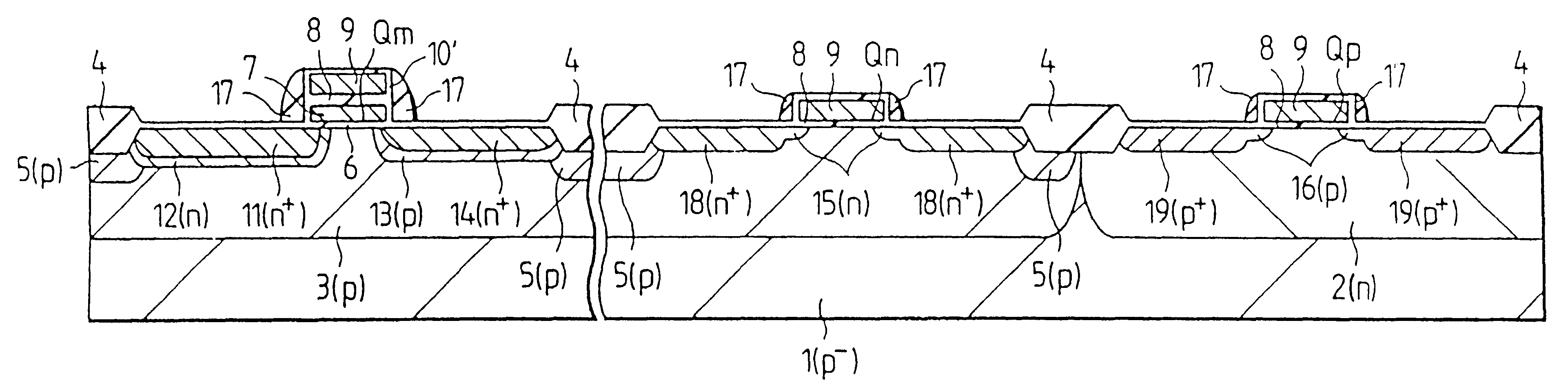
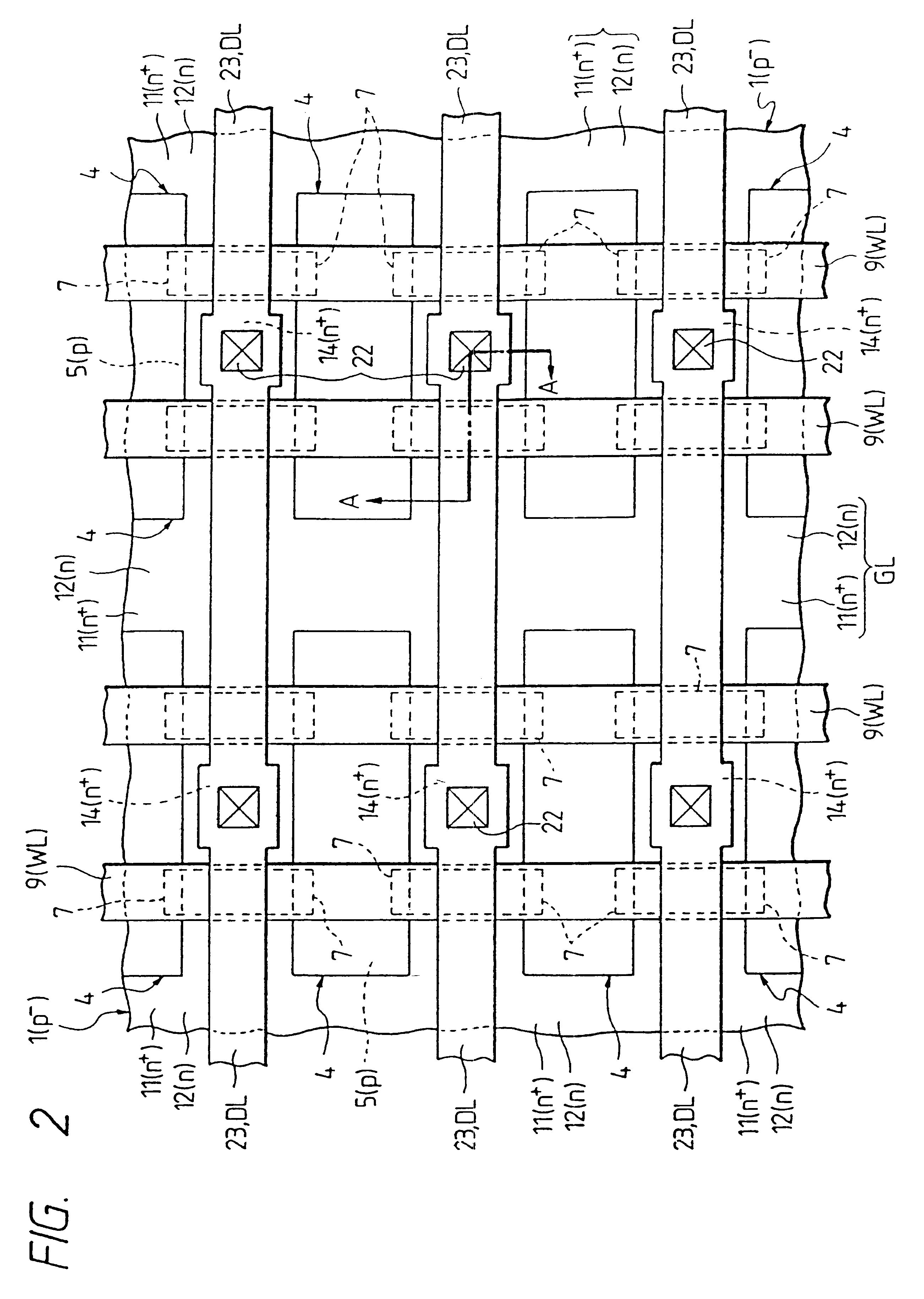
FIG. 3 is a sectional view of p-channel and n-channel MISFETs which constitute the memory cell and peripheral circuit of an EEPROM being the present invention. The section of the memory cell in FIG. 3 is taken along A--A in FIG. 2.

As shown in FIG. 3, the EEPROM is constructed using a p.sup.- -type semiconductor substrate 1 which is made of single-crystal silicon. A p-type well region 3 is provided in the principal surface part of the semiconductor substrate 1 in domains for forming the flash type nonvolatile memory cell Q.sub.m and the n-channel MISFET Q.sub.n while an n-type well region 2 is provided in a domain for forming the p-channel MISFET Q.sub.p.

An insulator film 4 for isolating the elements is provided between the adjacent domains for forming the elements, and on the principal surface parts of the n-type well region 2 and the p-type well region 3. In the principal surface part of the p-type well region 3, a p-type channel stopper region 5 is provided under the element isola...

second embodiment

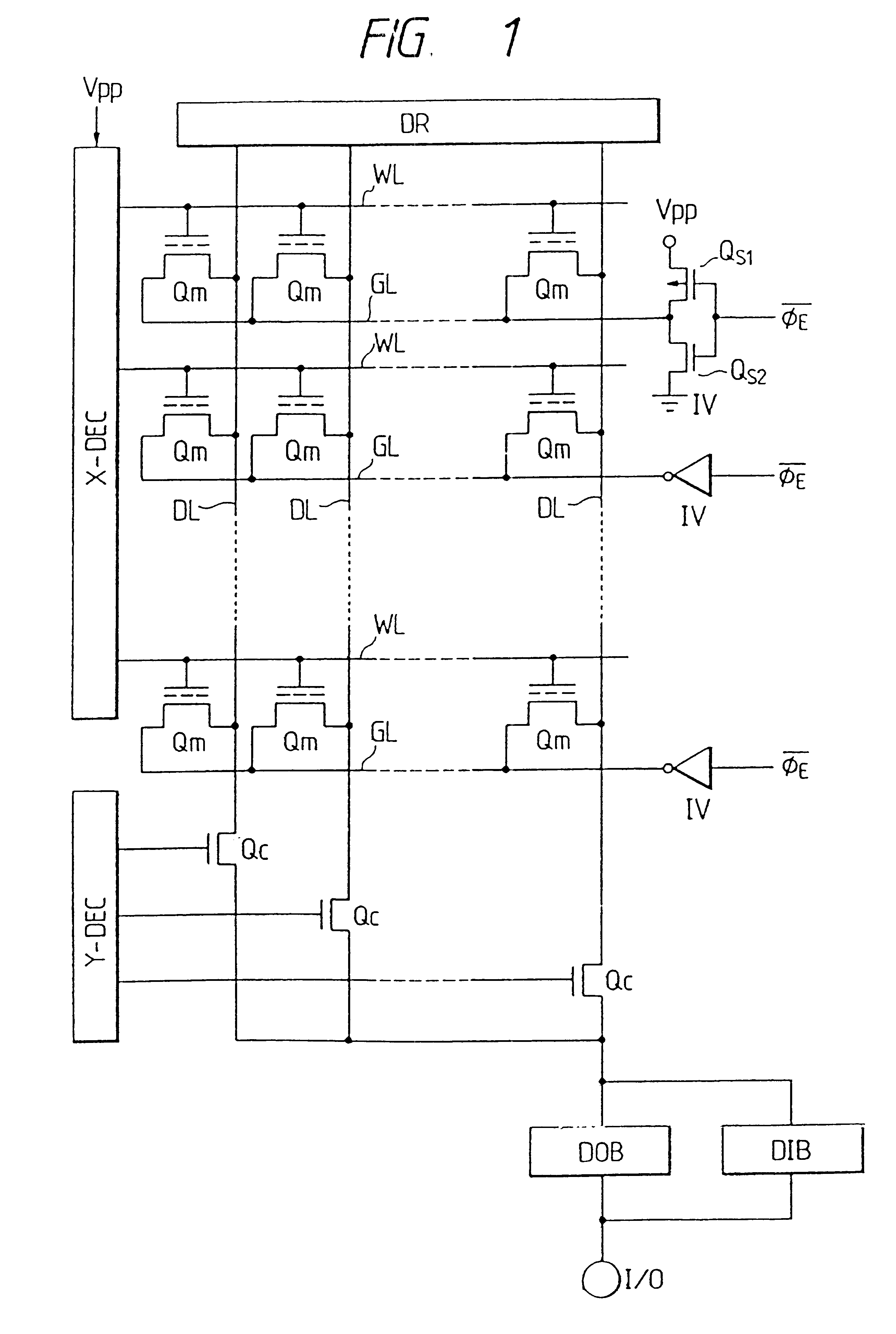
FIG. 20 shows the schematic construction of a flash type nonvolatile memory cell according to the present invention.

The point of difference from the first embodiment stated before will be described. In the flash type nonvolatile memory cell according to the second embodiment depicted in the Figure, a region 24 of low impurity concentration is locally formed in the vicinity of the part of the front surface of a source region 11 underlying one end of a floating gate electrode 7, thereby to form electric field buffer means for moderating an electric field which is established between the source region 11 and the end of the floating gate electrode 7 during the application of an erasing voltage.

That is, the electric field is moderated in such a way that a depletion layer is rendered liable to spread in the surface part of the source region 11 underlying the end of the floating gate electrode 7.

The low impurity concentration region 24 is formed in such a way that the amount of doping with...

third embodiment

Now, FIG. 31 shows a modification of the third embodiment stated above. A floating gate electrode 7 and a control gate electrode 9 are asymmetric between on the side of a source region 11, 12 and on the side of a drain region 14. In this case, the side of the floating gate electrode 7 near the source region 11, 12 is laterally protruded 0.2-0.3 [.mu.m] beyond the control gate electrode 9 by a side-wall spacer 17 in the same manner as in the foregoing embodiment. In contrast, on the side of the floating gate electrode 17 near the drain region 14, the ends of this electrode 17 and the control gate electrode 9 are vertically aligned so as to be substantially coplanar.

Owing to such an asymmetric structure, the overlap between the source region 11, 12 and the floating gate electrode 7 can be enlarged to enhance erasing characteristics, while at the same time, the overlap between the drain region 14 and the floating gate electrode 7 can be made null or small to enhance writing characteris...


PUM


Abstract

An EEPROM (Electrically Erasable Programmable Read Only Memory) has a structure in which the corners of a floating gate electrode of each memory cell MISFET near the source region thereof are rounded.The EEPROM is manufactured by a method characterized in that the ions of an impurity at a high dose are implanted in self-alignment with the floating gate electrode and control gate electrode of the memory cell MISFET so as to form the source and drain regions thereof, whereupon an oxidizing treatment is carried out.

Description

BACKGROUND OF THE INVENTIONThe present invention relates to a semiconductor integrated circuit device, and a method of manufacturing the same. More particularly, it relates to techniques which are effective when applied to a semiconductor integrated circuit device having a nonvolatile memory.A nonvolatile memory cell of the one-element type has been proposed as the nonvolatile memory cell of an EEPROM (Electrically Erasable Programmable Read Only Memory). This nonvolatile memory cell is constructed of a field-effect transistor (MISFET) which has a floating gate electrode (information storing gate electrode) and a control gate electrode (controlling gate electrode). The source region of the MISFET is connected to a source line, and the drain region to a data line.The nonvolatile memory cell is called a "flash type nonvolatile memory cell", in which information is written with hot electrons and is erased by tunneling. More specifically, the information writing operation of the nonvola...

Claims


Application Information

Patent Timeline
IPC IPC(8): H01L21/28H01L21/70H01L29/40H01L21/02H01L29/423H01L21/8247H01L27/105
CPCH01L27/105H01L29/42324H01L29/40114H10B41/40H10B41/49
Inventor KOMORI, KAZUHIROMEGURO, SATOSHINISHIMOTO, TOSHIAKIKUME, HITOSHIYAMAMOTO, HIDEAKI
Owner HITACHI LTD
Why Eureka
Try Eureka